17
\$\begingroup\$

I have read at numerous places that NAND gate is preferred over NOR gate in industry. The reasons given online say:

NAND has lesser delay than Nor due to the NAND PMOS (size 2 and in parallel) when compared to NOR PMOS (size 4 in series).

According to my understanding delay would be the same. This is how I think it works:

  • Absolute delay (Dabs) = t(gh+p)
  • g=logical effort
  • h=electrical effort
  • p=parasitic delay
  • t=delay unit which is technology constant

For NAND and NOR gate (gh+p) comes out to be (Cout/3 + 2). Also t is same for both. Then delay should be the same right?

\$\endgroup\$
4
  • 2
    \$\begingroup\$ If producing a "NOR" gate with the same driving capability requires use of transistors that are twice as big, what will that mean about the gate capacitance of those transistors, and how will that affect speed? \$\endgroup\$
    – supercat
    Commented May 16, 2014 at 23:05
  • \$\begingroup\$ At least for the HC family, TI lists identical propagation delays for the 74HC00 (NAND) and the 74HC02 (NOR) \$\endgroup\$
    – tcrosley
    Commented May 17, 2014 at 0:19
  • \$\begingroup\$ @placeholder Thanks for the clarification in your comment to my (now) deleted answer. It appears that the OP is referring to the internal design of IC's, and not any preference for logic designers to use one or the other, which is what I was mistakenly referring to. \$\endgroup\$
    – tcrosley
    Commented May 17, 2014 at 1:19
  • \$\begingroup\$ @tcrosley not a problem, may I suggest you are equipped to answer the problem? \$\endgroup\$ Commented May 17, 2014 at 2:24

2 Answers 2

25
\$\begingroup\$

1. NAND offers less delay.

As you were saying, the equation for delay is $$Delay = t(gh+p)$$ But the logical effort \$g\$ for NAND is less than that of NOR. Consider the figure showing 2 input CMOS NAND and NOR gate. The number against each transistor is a measure of size and hence capacitance. enter image description here
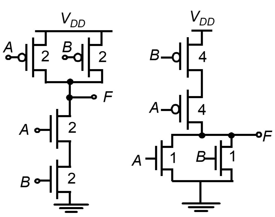
The logical effort can be calculated as \$g = C_{in}/3\$. Which gives

  • \$g = 4/3\$ for 2 input NAND and \$g = \frac{n+2}{3}\$ for n input NAND gate
  • \$g = 5/3\$ for 2 input NOR and \$g = \frac{2n+1}{3}\$ for n input NOR gate
  • refer wiki for table.

\$h=1\$ for a gate (NAND or NOR) driving the same gate and \$p=2\$ for both NAND and NOR. Hence NAND has lesser delay when compared with NOR.

EDIT: I have two more points to but and I am not 100% sure about the last point.

2. NOR occupies more area.

Adding the sizes of transistors in figure, it is clear that size of NOR is greater than that of NAND. And this difference in size will increase as the number of inputs are increased.

NOR gate will occupy more silicon area than NAND gate.

3. NAND uses transistors of similar sizes.

Considering the figure again, all the transistors in NAND gate have equal size where as NOR gates don't. Which reduces manufacturing cost of NAND gate. When considering gates with more inputs, NOR gates requires transistors of 2 different sizes whose size difference is more when comparing with NAND gates.

\$\endgroup\$
5
  • \$\begingroup\$ Your 3rd comment is simply a restating of the second comment. \$\endgroup\$ Commented May 17, 2014 at 15:49
  • \$\begingroup\$ @placeholder I'm not sure. Think this way: Assume that my circuit can be implemented either as '2 input NAND only' or as '2 input NOR only'. When designing the layout mask, it would be easier if my transistors are of same dimension. I can make mask by 'copy pasting' (or something like that). Time and effort and hence cost can be reduced. Correct me if its wrong. \$\endgroup\$
    – nidhin
    Commented May 17, 2014 at 16:40
  • \$\begingroup\$ For the 1st answer you said say for 2 input gates g(NAND)=4/3 and g(NOR)=5/3. But h(NAND)=Cout/Cin=Cout/4 and h(NOR)=Cout/5. and Also P(NAND and NOR)=Cpt/Cinv=6/3=2. So d(NAND,NOR)=gh+p=(Cout/3)+2.. \$\endgroup\$
    – Curious
    Commented May 17, 2014 at 23:10
  • \$\begingroup\$ Oh I get it now. When we drive one nand with another h=1 and similarly nor driving another nor h=1. Then yes delay of nand would be 10/3 and for nor it will be 11/3. Thanks a ton :) \$\endgroup\$
    – Curious
    Commented May 17, 2014 at 23:21
  • \$\begingroup\$ Can you explain the difference in logical effort required for the n and p channel CMOS MOFSETs? It appears they are the same type in both NAND and NOR circuits. If not, can you explain each type further? \$\endgroup\$
    – notaorb
    Commented Sep 19, 2023 at 5:26
8
\$\begingroup\$

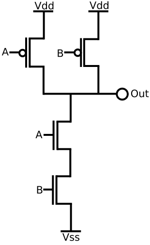
Roughly speaking, Nmos transistors allow double the current per channel area compared to Pmos transistors. You can think about it as if the Nmos has half the resistance of an equal sized Pmos. The way the Cmos Nand topology is, it lends itself to having more equal sizes of transistors as you can see from here:
enter image description here

If either input is low, a single Pmos resistance drives the output high. If both inputs are high, then there's 2 Nmos resistances (~=1 Pmos resistance). If all of the transistors are the same minimum size of a technology node, then this topology is ideal because whether you're driving the output high or low, the resistance to ground or Vdd is the same.

Lastly, the reason Pmos transistors don't fair as well as Nmos's is due to the lower carrier mobility of holes which are the majority carrior of a PMOS. Nmos's majority carrier are electrons which have significantly better mobility.

Also, don't confuse Nand Flash with Nand Cmos. Nand Flash memory is also more popular, but that's for different reasons.

\$\endgroup\$
1
  • \$\begingroup\$ I think answer would be improved if you talk about the relative loading (gate area) and the relative transconductance and thus the speed g_m/C. \$\endgroup\$ Commented May 17, 2014 at 3:36

Not the answer you're looking for? Browse other questions tagged or ask your own question.