4
\$\begingroup\$

I am trying to learn how differential amplifiers work, and I would like to be able to visualize how the voltages and currents stabilize if the input voltages are changed. Specifically, I'm caught up on the circular dependency between the currents going through either transistor Q1 or Q2, and the source terminal voltage which is connected for them.

diff-amp

I do understand that what's happening with the shared source voltage is its changing to be in balance with the currents coming through the transistors (which is capped by the source current below). But I'm used to thinking in terms of one transistor, where I deduce the current from knowing the terminal voltages. In this case, it seems to be the source terminal voltage follows from the currents, but the currents also still follow from the voltage \$v_{GS}\$ which is a function of \$v_{IN}\$ (fixed) and \$v_{S}\$ (not fixed).

I tried solving for this source terminal voltage to see if this would shed any insight but the result was messy:

$$I_S =I_1 + I_2$$

$$i_{D1} = \frac{K}{2}(v_{GS1}-V_T)^2$$

which is equal to:

$$\frac{K}{2}(v_{GS1}-V_T)^2 = \frac{K}{2}((v_{IN1}-V_T)-v_{S})^2$$

and so the same for the other transistor

$$i_{D2} = \frac{K}{2}((v_{IN2}-V_T)-v_{S})^2$$

combining these and solving for the quadratic equation, I got:

$$ v_{S} = \frac{2(v_{IN1} + v_{IN2} - 2V_T) \pm \sqrt{(2(v_{IN1} + v_{IN2})^2 - 8(\frac{2 I_S}{K}-(v_{IN1}-V_T)^2-(v_{IN2}-V_T)^2))}}{4} $$

This didn't really help me get a much better sense of what's happening.

What I'd like

is to be able to roughly imagine how the electric fields propagate from the disturbance (change in either voltage input), in order to understand how the circuit arrives at a new equilibrium.

\$\endgroup\$

3 Answers 3

3
\$\begingroup\$

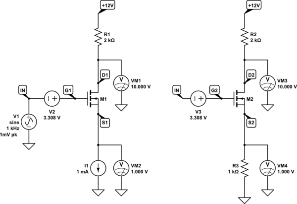
When you say you're familiar with a single transistor arrangement, do you mean with a current source, or with a resistor at the FET's source terminal? The two are wildly different in behaviour:
schematic

simulate this circuit – Schematic created using CircuitLab

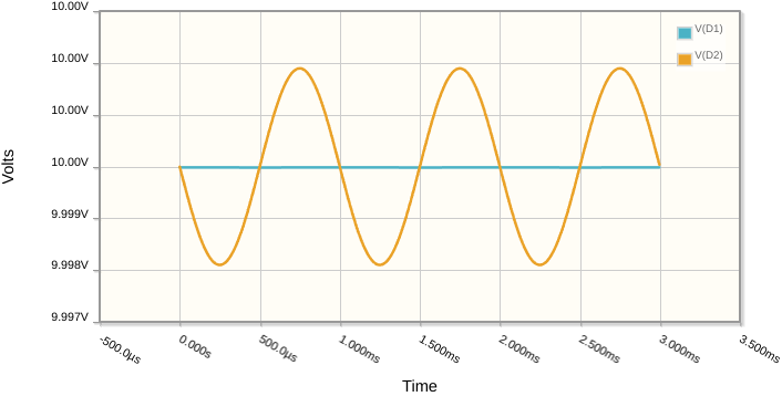
Those two circuits are biased identically, and yet their response to changes in \$V_{IN}\$ (from the 1mV AC source V1) is completely different:
enter image description here

The circuit on the left has no voltage gain, because drain current is constant, 1mA, and the voltage across R1 never changes. The only way you can get \$V_{D1}\$ to change is by changing source current, and that can't happen in the single transistor arrangement on the left.

We may also assume, for the left circuit, that \$V_{GS1} = V_{G1} - V_{S1}\$ will be constant regardless of input potential \$V_{IN}\$ (and \$V_{G1}\$), because drain current \$I_{D1}\$ never changes. M1 is acting as a perfect source-follower, in which \$V_{S1}\$ rises and falls in perfect unison with \$V_{G1}\$.

However, when you place two of those back to back, in a long tailed pair sharing the same current source, drain current can change:
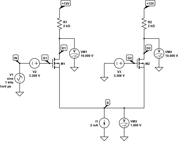
schematic

simulate this circuit

I've doubled source current, which by symmetry is shared equally in both FET channels, so DC conditions are identical on both sides to the single transistor setup.

However, source potential \$V_S\$ is now common to both transistors, so when one changes, so does the other.


It's difficult (at least for me) to intuit what happens to \$V_S\$ when gate potentials \$V_{G1}\$ and \$V_{G2}\$ are perturbed with respect to each other, causing that convenient symmetry to be lost. Before, we were able to say that \$V_{GS}\$ was constant, because \$V_{S1}\$ "followed" \$V_{G1}\$, but here we cannot.

As long as we are dealing with small perturbations, so that drain current \$I_D\$ doesn't change too much, we can assume that FET transconductance \$g_m\$ remains constant. This is the change in drain current \$I_D\$ in response to changes in \$V_{GS}\$. Change in drain current \$\Delta I_{D1}\$ will have this relationship to change in gate-source potential difference \$\Delta V_{GS1}\$:

$$ \Delta I_{D1} = g_m \cdot \Delta V_{GS1} $$

Instead of having \$\Delta\$ symbols everywhere, I'll use lower-case variable names, to indicate small changes, AC signals.

$$ \begin{aligned} i_{D1} &= g_m \cdot v_{GS1} \\ \\ &= g_m \cdot (v_{G1} - v_S) \\ \\ \end{aligned} $$

Similarly, for M2 we have:

$$ i_{D2} = g_m \cdot (v_{G2} - v_S) $$

By KCL, the sum of drain currents must equal source I1:

$$ I_{D1} + I_{D2} = I_1 $$

Since we are dealing with AC, changes in potential and current, and since \$I_1\$ is not changing, this becomes:

$$ \begin{aligned} i_{D1} + i_{D2} &= \Delta I_1 = 0 \\ \\ g_m \cdot (v_{G1} - v_S) + g_m \cdot (v_{G2} - v_S) &= 0 \\ \\ v_{G1} - v_S + v_{G2} - v_S &= \frac{0}{g_m} \\ \\ -2v_S + v_{G1} + v_{G2} &= 0 \\ \\ v_S &= \frac{1}{2}(v_{G1} + v_{G2}) \end{aligned} $$

If we hold one input steady while we increase the other by \$\Delta V\$, we can expect \$V_S\$ to rise by \$\frac{\Delta V}{2}\$.

Going back to our simulation, in which I am applying a 1mV peak (or 2mV peak-to-peak) sinusoid to IN, while I keep G2 at a fixed potential, I would expect \$V_S\$ to vary by half the amount that \$V_{IN}\$ varies:
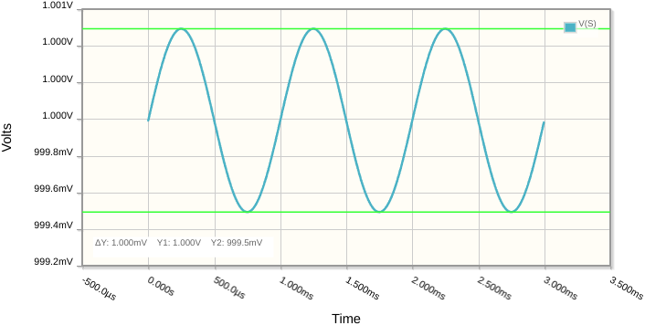
enter image description here


To finish off the analysis, we've found so far:

$$ \begin{aligned} i_{D1} &= g_m (v_{G1} - v_S) \\ \\ i_{D2} &= g_m (v_{G2} - v_S) \\ \\ \end{aligned} $$

and

$$ v_S = \frac{1}{2}(v_{G1} + v_{G2}) $$

Combining those, we get:

$$ \begin{aligned} i_{D1} &= g_m \left(v_{G1} - \frac{1}{2}(v_{G1} + v_{G2}) \right) \\ \\ &= g_m \left( \frac{v_{G1}}{2} - \frac{v_{G2}}{2} \right) \\ \\ &= \frac{g_m}{2} ( v_{G1} - v_{G2} ) \\ \\ \end{aligned} $$

For M2, the result is similar, with \$v_{G1}\$ and \$v_{G2}\$ swapped:

$$ i_{D2} = \frac{g_m}{2} ( v_{G2} - v_{G1} ) $$

Lastly we find the output voltages \$v_{D1}\$ and \$v_{D2}\$. These are trivial to calculate, since they depend only on changing drain current \$I_D\$ through drain resistances \$R_D\$. We just need to apply Ohm's law:

$$ \begin{aligned} i_{D1} &= \frac{v_{D1}}{R_D} \\ \\ i_{D2} &= \frac{v_{D2}}{R_D} \\ \\ \end{aligned} $$

Substituting \$i_{D1}\$ and \$i_{D2}\$:

$$ \begin{aligned} \frac{v_{D1}}{R_D} &= \frac{g_m}{2} ( v_{G1} - v_{G2} ) \\ \\ \frac{v_{D2}}{R_D} &= \frac{g_m}{2} ( v_{G2} - v_{G1} ) \\ \\ \end{aligned} $$

These are the output voltages, then, in terms of inputs \$V_{G1}\$ and \$V_{G2}\$, and transconductance \$g_m\$:

$$ \begin{aligned} v_{D1} &= \frac{g_mR_D}{2} ( v_{G1} - v_{G2} ) \\ \\ v_{D2} &= \frac{g_mR_D}{2} ( v_{G2} - v_{G1} ) \\ \\ \end{aligned} $$

Differential gain \$A\$ is:

$$ \begin{aligned} A &= \frac{v_{D2}-v_{D1}}{v_{G2}-v_{G1}} \\ \\ &= \frac{\frac{g_mR_D}{2} ( v_{G2} - v_{G1} ) - \frac{g_mR_D}{2} ( v_{G1} - v_{G2} )}{v_{G2}-v_{G1}} \\ \\ &= \frac{g_mR_D}{2} \frac{( v_{G2} - v_{G1} - v_{G1} + v_{G2} ) }{v_{G2}-v_{G1}} \\ \\ &= \frac{g_mR_D}{2} \frac{(2v_{G2} - 2v_{G1}) }{v_{G2}-v_{G1}} \\ \\ &= g_mR_D \\ \\ \end{aligned} $$

I don't remember ever having derived this result for myself, I always just trusted the books. It's very satisfying to have finally done it, so thanks for asking!

\$\endgroup\$
1
\$\begingroup\$

But I'm used to thinking in terms of one transistor ...

If you are happy with analysing a single transistor, then I would suggest breaking this circuit apart into its Common Mode, and Differential Mode, modes of operation.

For the Differential mode, draw a line of symmetry between the two sources. The point between the sources always stays at zero signal volts, as when Vin1 rises, Vin2 falls (the definition of differential). Now you have an effectively grounded source, and you can analyse either transistor by itself.

For the common mode, put the two transistors in parallel, connect Vin1 to Vin2, put R1 and R2 in parallel. Analyse what happens to that 'single transistor'.

A little thought will show that any arbitrary combination of Vin1 and Vin2 inputs can be broken down into a common mode and a differential mode part. Analyse each, then add them together for the actual output.

\$\endgroup\$
1
\$\begingroup\$

Basic idea

It can be revealed at а functional level by equivalent electrical circuits. In this brilliant circuit solution initially called with the figurative name "long-tailed pair", a total of three sources - two voltage and one current - interact like living beings. In some cases they help each other and in others they oppose each other like people in the game tug of war.

Implementation

The two voltage sources are implemented by the source followers Q1 and Q2. The current source (or, more precisely speaking, current sink) is implemented by another transistor (not shown in the OP's circuit). So these sources are not actually true sources (producing power) but dynamic resistors that only regulate voltage and current (see more about this approach in another related question and answer of mine).

Conceptual circuit

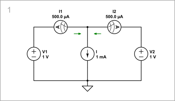
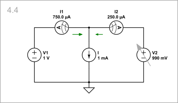
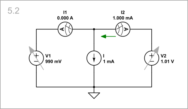
To simulate the circuit, actually we have to connect three sources in parallel. The problem is that "ideal" voltage sources should not be connected in parallel because even with the smallest difference in their voltages, a high current will flow between them (that is why CircuitLab does not allow it). To mitigate the conflict between them, we need to insert small resistances in series. For this purpose, we can use ammeters with some, albeit small, internal resistance (I have set 20 Ω). They will serve as current outputs, and the voltage drops across them can be used as voltage outputs.

schematic

simulate this circuit – Schematic created using CircuitLab

Operation

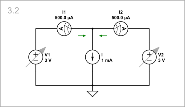
Using this modest setup we will be able to explore all circuit modes. The elements whose quantities we vary as inputs are indicated by an arrow in light gray. Initially, V1 = V2 and the bias 1 mA current splits into two 0.5 mA currents that flow through the sources.

Biasing mode

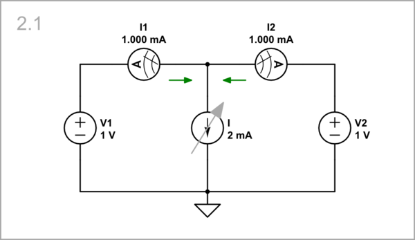
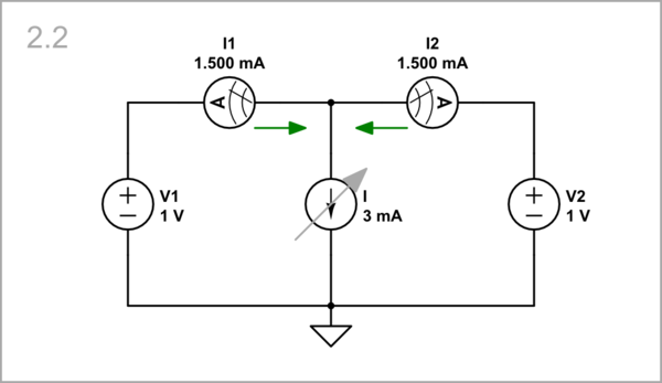
One of the basic ideas of the differential pair is that the transistors are biased on the emitter side. This is done via a current source (I) because the emitters are not firmly fixed ("immovable") but "shift" when both input voltages change simultaneously in the so-called "common mode". In this way, the bias current will not change when the emitter voltage varies. Initially the bias current is adjusted to 1 mA but let's experiment with two more values of 2 and 3 mA to see how the sources react.

I = 2 mA: When we increase the bias current with 1 mA, the voltage does not change because it is set by two constant voltage sources in parallel...

schematic

simulate this circuit

I = 3 mA: ... also if we increase it by another 1mA and continue in the same vein.

schematic

simulate this circuit

So, in this mode, the two voltage sources cooperate to keep the voltage constant when the current source changes the common current. In this way, they provide ideal load conditions (no voltage variations) for the current source; they act as an "ideal current load".

Reaching equilibrium: In the real (OP's) circuit, the two voltage sources in parallel are implemented as negative feedback circuits (emitter followers). The current source disturbs their outputs and they react to this intervention by simultaneously changing their input gate-source voltages Vgs. The equilibrium is reached when the relation between I and Vgs corresponds to the transistor transfer characteristic.

"Reversed transistor": In this mode, a unique phenomenon of "reversal" through negative feedback is observed. As we all know, the gate-source voltage is the input quantity and the drain (emitter) current is the output quantity. However, here it is reversed - the current is the input quantity, and the voltage Vgs is the output quantity. This is done by the transistor adjusting (via the negative feedback mechanism) its input voltage to match the output current. As a result, the current becomes the input quantity and the voltage Vgs the output quantity. This is not only electrical but a universal phenomenon that we can observe all around us.

Common mode

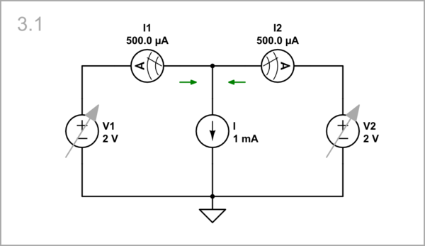
The differential amplifier is designed with two inputs to be able to distinguish harmful (common-mode) from useful (differential-mode) signals. Let's first examine how the circuit reacts to the former. For this purpose, we have to change simultaneously both input voltages in the same way.

V1 = V2 = 2 V: We see that if we increase the voltage by 1 V...

schematic

simulate this circuit

V1 = V2 = 3 V: ... and by another 1 V, the current does not change.

schematic

simulate this circuit

So, in this mode, the two voltage sources cooperate to change the voltage while the current source keeps the common current constant. In this way, the current source provides ideal load conditions (no current variations) for the voltage sources; it acts as an "ideal voltage load".

Single-ended mode

This is an intermediate mode in which we change only one input voltage and keep the other constant. It is asymmetrical and less often used.

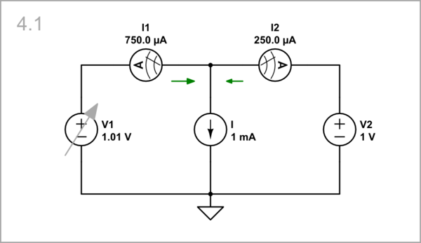
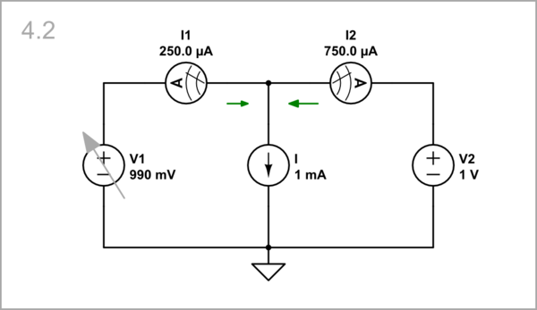
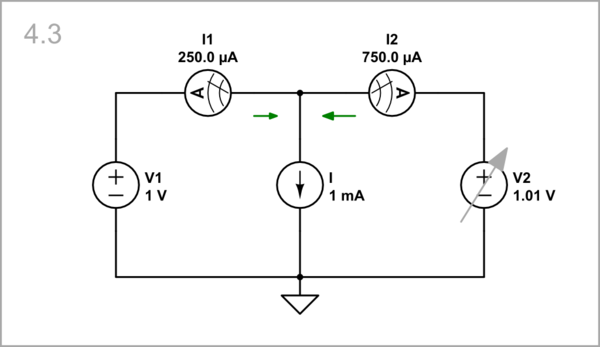
Increasing V1: I1 increases, I2 decreases.

schematic

simulate this circuit

Decreasing V1: I1 decreases, I2 increases.

schematic

simulate this circuit

Increasing V2: I2 increases, I1 decreases.

schematic

simulate this circuit

Decreasing V2: I2 decreases, I1 increases.

schematic

simulate this circuit

So, in this mode, one voltage source resists "passively" when the other tries to change the voltage at the common point of the emitters. The current source is not involved in this.

Differential mode

This is the main (symmetrical and most used) mode in which we change both input voltages but in opposite directions. The two voltage sources actively resist each other while the current source passively "observes" .

Increasing V1, decreasing V2: As you can see, it only takes 10 mV to change the voltages in one direction...

schematic

simulate this circuit

Decreasing V1, increasing V2: ... or the other...

schematic

simulate this circuit

... and the bias current is diverted from one voltage source to the other.

\$\endgroup\$

Your Answer

By clicking “Post Your Answer”, you agree to our terms of service and acknowledge you have read our privacy policy.

Not the answer you're looking for? Browse other questions tagged or ask your own question.