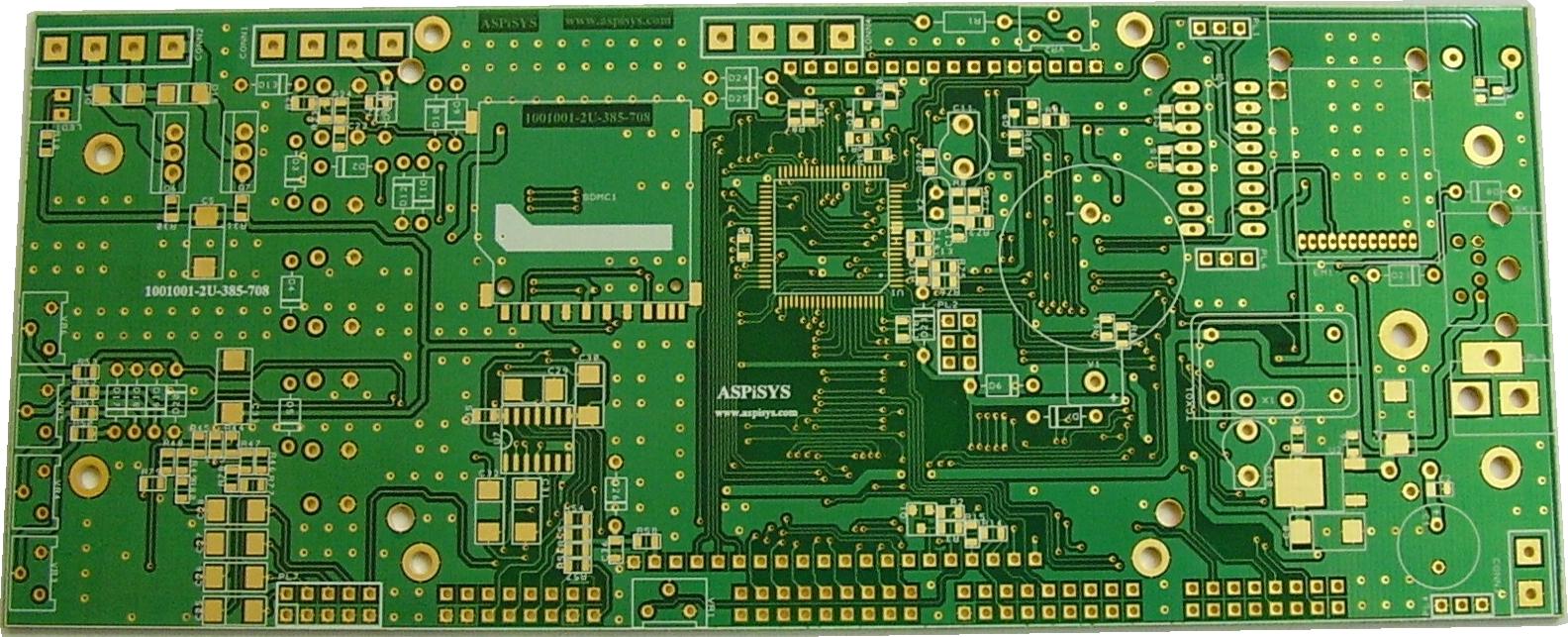
I'm designing a PCB for USB 3.0, the specifications for DifferantialDifferential impedance comes at 90 ohms with a tolleancetolerance of +- 5 ohms.
I've used different calculation tools but when I have to hold these specs my traces arare really wide in comparison to the usb3.0 printed circuits that I have as example, even with the same PCB material.
I searched the internetInternet and found some specs for the widenesswidth and spacing but if I put them inthose into the calculation tool I'm atit shows 170 ohms..
Anyone have an idea how manufacturers solve this?
I also had a question to manufacturerabout manufacturers putting multiple Vias from top layer to bottom layer. In the past I read some articles about this but can't seem to remember what it's for, anyone have an idea about that?
Here is an example : http://www.aspisys.com/netqe128.jpg
Thanks
Kind Regards
Joris Aerts
