added 983 characters in body
Source Link
sherrellbc
  • 3.5k
  • 7
  • 37
  • 63

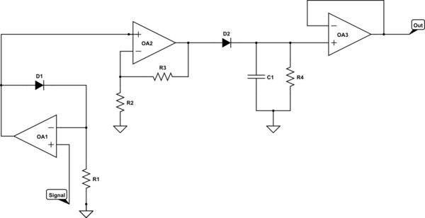
Although what you have presented above uses fewer components and even has the added benefit of mains isolation, another detection circuit that I know of is presented below. Perhaps with added mains isolation between the second stage amp and the peak detector then this circuit could be of use.
schematic

simulate this circuit – Schematic created using CircuitLab

This circuit is generally used as a small signal detector by using an ideal diode op-amp configuration, amplification stage, and a peak detector fed into a buffer. You could possibly make the second stage an attenuator instead.


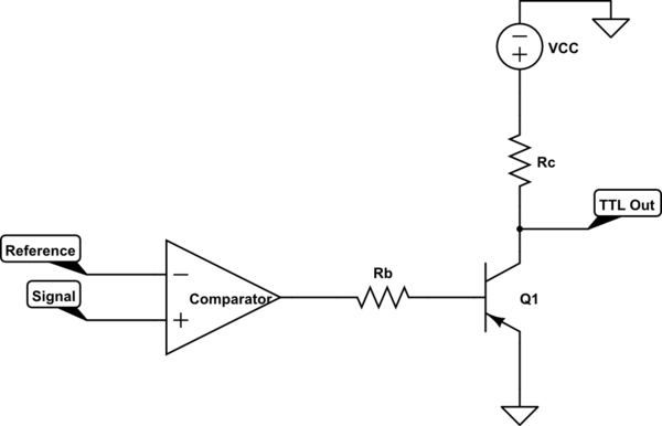
Or something as simple as a comparator, assuming you have appropriately conditioned the mains signal (AC-DC conversion, for example), and a PNP transistor to convert the positive and negative rail voltages that you would get at the output of an op-amp comparator:
schematic

simulate this circuit

In this case, when the conditioned signal is greater than the reference the Op-Amp will rail high and turn the PNP off. In the off state, the TTL_OUT node will be pulled-high through Rc. Likewise, when the signal is less than the reference the Op-Amp will rail low and turn the PNP on. You must design Rb and Rc such that in this situation the transistor will saturate and thereby drive the TTL_OUT node to saturation (~200mV).

Although what you have presented above uses fewer components and even has the added benefit of mains isolation, another detection circuit that I know of is presented below. Perhaps with added mains isolation between the second stage amp and the peak detector then this circuit could be of use.

schematic

simulate this circuit – Schematic created using CircuitLab

This circuit is generally used as a small signal detector by using an ideal diode op-amp configuration, amplification stage, and a peak detector fed into a buffer. You could possibly make the second stage an attenuator instead.


Or something as simple as a comparator, assuming you have appropriately conditioned the mains signal (AC-DC conversion, for example), and a PNP transistor to convert the positive and negative rail voltages that you would get at the output of an op-amp comparator:

schematic

simulate this circuit

In this case, when the conditioned signal is greater than the reference the Op-Amp will rail high and turn the PNP off. In the off state, the TTL_OUT node will be pulled-high through Rc. Likewise, when the signal is less than the reference the Op-Amp will rail low and turn the PNP on. You must design Rb and Rc such that in this situation the transistor will saturate and thereby drive the TTL_OUT node to saturation (~200mV).

Source Link
sherrellbc
  • 3.5k
  • 7
  • 37
  • 63

Although what you have presented above uses fewer components and even has the added benefit of mains isolation, another detection circuit that I know of is presented below. Perhaps with added mains isolation between the second stage amp and the peak detector then this circuit could be of use.

schematic

simulate this circuit – Schematic created using CircuitLab

This circuit is generally used as a small signal detector by using an ideal diode op-amp configuration, amplification stage, and a peak detector fed into a buffer. You could possibly make the second stage an attenuator instead.