replaced http://electronics.stackexchange.com/ with https://electronics.stackexchange.com/
Source Link

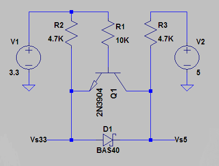
From the cheap[er?] solution department, the FET (from the accepted answer based on the NXP appnote) can be replaced with a BJT and Schottky diode as in Silicon Labs AN883. Their schematic is a bit complicated with other things, so I've extracted the essential bit here and reoriented it so it looks like in the accepted answer for easy comparison of the two schematics:

enter image description here

The BJT does translation in the low->high direction only... exactly as discussed in Single transistor level up shifterSingle transistor level up shifter. The Schottky replaces the body diode of the FET for the high->low translation.

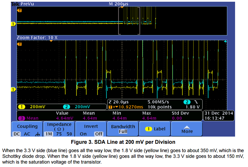
Below is their zoomed in scope measurement for a 3.3<->1.8V translator; they also propose this schematic for 5<->1.8V translation etc. When doing 3.3<->1.8V translation a MMBT3904 had only 150mV (saturation) drop. The BAS40 diode had 350mV drop in the opposite direction. These offesets affect (obviously) the logic-low level output on the low and respectively high side of the translator.

enter image description here

They had nice CMOS devices on both sides, so input impedance wasn't much of an issue. There was no visible degradation/offset of the logic-high margins in their 1V/div trace, so I haven't bothered including it here. The input impedance of their devices were at least 1Mohm from what I can tell from a simulation. Logic-high margins start to degrade below 100K input impedance or so.

Also, they recommend this BJT-based translator only up to 300KHz or so.

I'm not sure which of these solutions is cheaper in practice, FET or Schottky + BJT... but this one certainly needs more parts... unless you use one of those diode+transistor packages, which do exist, e.g. PZMT1101. But you also need 3 resistors.

From the cheap[er?] solution department, the FET (from the accepted answer based on the NXP appnote) can be replaced with a BJT and Schottky diode as in Silicon Labs AN883. Their schematic is a bit complicated with other things, so I've extracted the essential bit here and reoriented it so it looks like in the accepted answer for easy comparison of the two schematics:

enter image description here

The BJT does translation in the low->high direction only... exactly as discussed in Single transistor level up shifter. The Schottky replaces the body diode of the FET for the high->low translation.

Below is their zoomed in scope measurement for a 3.3<->1.8V translator; they also propose this schematic for 5<->1.8V translation etc. When doing 3.3<->1.8V translation a MMBT3904 had only 150mV (saturation) drop. The BAS40 diode had 350mV drop in the opposite direction. These offesets affect (obviously) the logic-low level output on the low and respectively high side of the translator.

enter image description here

They had nice CMOS devices on both sides, so input impedance wasn't much of an issue. There was no visible degradation/offset of the logic-high margins in their 1V/div trace, so I haven't bothered including it here. The input impedance of their devices were at least 1Mohm from what I can tell from a simulation. Logic-high margins start to degrade below 100K input impedance or so.

Also, they recommend this BJT-based translator only up to 300KHz or so.

I'm not sure which of these solutions is cheaper in practice, FET or Schottky + BJT... but this one certainly needs more parts... unless you use one of those diode+transistor packages, which do exist, e.g. PZMT1101. But you also need 3 resistors.
From the cheap[er?] solution department, the FET (from the accepted answer based on the NXP appnote) can be replaced with a BJT and Schottky diode as in Silicon Labs AN883. Their schematic is a bit complicated with other things, so I've extracted the essential bit here and reoriented it so it looks like in the accepted answer for easy comparison of the two schematics:

enter image description here

The BJT does translation in the low->high direction only... exactly as discussed in Single transistor level up shifter. The Schottky replaces the body diode of the FET for the high->low translation.

Below is their zoomed in scope measurement for a 3.3<->1.8V translator; they also propose this schematic for 5<->1.8V translation etc. When doing 3.3<->1.8V translation a MMBT3904 had only 150mV (saturation) drop. The BAS40 diode had 350mV drop in the opposite direction. These offesets affect (obviously) the logic-low level output on the low and respectively high side of the translator.

enter image description here

They had nice CMOS devices on both sides, so input impedance wasn't much of an issue. There was no visible degradation/offset of the logic-high margins in their 1V/div trace, so I haven't bothered including it here. The input impedance of their devices were at least 1Mohm from what I can tell from a simulation. Logic-high margins start to degrade below 100K input impedance or so.

Also, they recommend this BJT-based translator only up to 300KHz or so.

I'm not sure which of these solutions is cheaper in practice, FET or Schottky + BJT... but this one certainly needs more parts... unless you use one of those diode+transistor packages, which do exist, e.g. PZMT1101. But you also need 3 resistors.

Source Link

From the cheap[er?] solution department, the FET (from the accepted answer based on the NXP appnote) can be replaced with a BJT and Schottky diode as in Silicon Labs AN883. Their schematic is a bit complicated with other things, so I've extracted the essential bit here and reoriented it so it looks like in the accepted answer for easy comparison of the two schematics:

enter image description here

The BJT does translation in the low->high direction only... exactly as discussed in Single transistor level up shifter. The Schottky replaces the body diode of the FET for the high->low translation.

Below is their zoomed in scope measurement for a 3.3<->1.8V translator; they also propose this schematic for 5<->1.8V translation etc. When doing 3.3<->1.8V translation a MMBT3904 had only 150mV (saturation) drop. The BAS40 diode had 350mV drop in the opposite direction. These offesets affect (obviously) the logic-low level output on the low and respectively high side of the translator.

enter image description here

They had nice CMOS devices on both sides, so input impedance wasn't much of an issue. There was no visible degradation/offset of the logic-high margins in their 1V/div trace, so I haven't bothered including it here. The input impedance of their devices were at least 1Mohm from what I can tell from a simulation. Logic-high margins start to degrade below 100K input impedance or so.

Also, they recommend this BJT-based translator only up to 300KHz or so.

I'm not sure which of these solutions is cheaper in practice, FET or Schottky + BJT... but this one certainly needs more parts... unless you use one of those diode+transistor packages, which do exist, e.g. PZMT1101. But you also need 3 resistors.