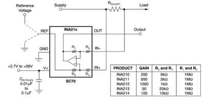
Showing eg Vcc = 2.5V to 5.5V means that the IC will operate correctly from ANY voltage in the 2.5V - 5.5V range.
That is, the voltage range shown for V+ is not REQUIRED - it is allowed. For the TI part the 2.7V to 26V notation means that the IC can operate from a supply voltage of 2.7V to 26V. The output voltage is essentially unchanged by varying V+, except that V+ needs to be >= Vout - see data sheet for details.
_____________________________
The reference voltage in this example product diagram that you provided is not directly related to the measurement process. The voltage on pin "REF" is the voltage that the output voltage is relative to. This allows the IC to be used eg in a system with an artificially generated ground that is above true ground potential. In most cases you want Vout to be relative to true ground so "REF" is grounded, as shown.
________________________________
There are many web examples. Commercial products often contain block diagrams which help greatly in understanding.
A low side circuit is easy to use IF you are able to insert a sensor in the ground lead.
A high side sensor is useful when the ground must be continuous from panel to load.
Essentially high side sensors drop a small voltage across a reference "shunt" of known resistance and use an amplifier to create a ground based amplified.
Have a look at these - each image links to a relevant page. Some are tutorials with much detail. Some use custom ICs, some are discrete. Look at a few of the tutorials and you should be well on the way to a solution. Or in text form.
Examples:
LT1999 but gives general idea.
LTC6101 look at block diagram.
Maxim tutorial
MAX4172 look at block diagram.

