Post Closed as "Needs details or clarity" by brhans, Daniel Grillo, pipe, Neil_UK, jms
edited body
Source Link
cnmesr
  • 113
  • 7

CPU has generated this sequence of logic addresses (in decimal):

777, 2047, 1199, 1100, 546, 129, 3201

page size is 512 Byte, CPU generates logic addresses, 12 Bit length, main memory has 4 pages.

I understand the following table: We just converted the decimal addresses to binary. The total address length is 12 Bit. From task we know that page size is 512 Byte, so 2^9 Byte = 9 Bit for offset. 12 Bit - 9 Bit = 3 Bit for page. So first 3 Bits are page and the other remaining 9 Bit are offset. Easy so far.

enter image description here

But here comes the second part of the task and I don't understand how the table was made...

Make a table that illustrates the content of the table above (called MMU) after each finished memory access in the same order shown above. You only need to specify the necessary entries (so if there is same page twice, ignore the duplicate). At the beginning, all page frames are unassigned and they are used with an ascending page number. If all page frames are in use, the LRU replacement takes place.

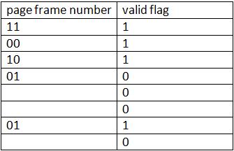
Here is the solution of the table but I don't understand... That's my question, how was this table created? I don't get the logic.

enter image description here

Edit: For second table I can see task said 4 pages. So we have 00, 01, 10, 11(so in decimal 0, 1, 2, 3) but why they did it in that order in the table? That's what I don't understand.

Edit: I don't understand the order of the second table. Why did we start with 11, then 00, then 10 etc. It doesn't make sense for me...

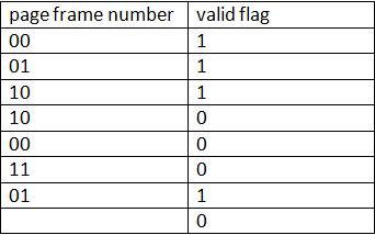
Here is how I would have filled the table:

enter image description hereenter image description here

What do you think?

CPU has generated this sequence of logic addresses (in decimal):

777, 2047, 1199, 1100, 546, 129, 3201

page size is 512 Byte, CPU generates logic addresses, 12 Bit length, main memory has 4 pages.

I understand the following table: We just converted the decimal addresses to binary. The total address length is 12 Bit. From task we know that page size is 512 Byte, so 2^9 Byte = 9 Bit for offset. 12 Bit - 9 Bit = 3 Bit for page. So first 3 Bits are page and the other remaining 9 Bit are offset. Easy so far.

enter image description here

But here comes the second part of the task and I don't understand how the table was made...

Make a table that illustrates the content of the table above (called MMU) after each finished memory access in the same order shown above. You only need to specify the necessary entries (so if there is same page twice, ignore the duplicate). At the beginning, all page frames are unassigned and they are used with an ascending page number. If all page frames are in use, the LRU replacement takes place.

Here is the solution of the table but I don't understand... That's my question, how was this table created? I don't get the logic.

enter image description here

Edit: For second table I can see task said 4 pages. So we have 00, 01, 10, 11(so in decimal 0, 1, 2, 3) but why they did it in that order in the table? That's what I don't understand.

Edit: I don't understand the order of the second table. Why did we start with 11, then 00, then 10 etc. It doesn't make sense for me...

Here is how I would have filled the table:

enter image description here

What do you think?

added 295 characters in body
Source Link
cnmesr
  • 113
  • 7

CPU has generated this sequence of logic addresses (in decimal):

777, 2047, 1199, 1100, 546, 129, 3201

page size is 512 Byte, CPU generates logic addresses, 12 Bit length, main memory has 4 pages.

I understand the following table: We just converted the decimal addresses to binary. The total address length is 12 Bit. From task we know that page size is 512 Byte, so 2^9 Byte = 9 Bit for offset. 12 Bit - 9 Bit = 3 Bit for page. So first 3 Bits are page and the other remaining 9 Bit are offset. Easy so far.

enter image description here

But here comes the second part of the task and I don't understand how the table was made...

Make a table that illustrates the content of the table above (called MMU) after each finished memory access in the same order shown above. You only need to specify the necessary entries (so if there is same page twice, ignore the duplicate). At the beginning, all page frames are unassigned and they are used with an ascending page number. If all page frames are in use, the LRU replacement takes place.

Here is the solution of the table but I don't understand... That's my question, how was this table created? I don't get the logic.

enter image description here

Edit: For second table I can see task said 4 pages. So we have 00, 01, 10, 11(so in decimal 0, 1, 2, 3) but why they did it in that order in the table? That's what I don't understand.

Edit: I don't understand the order of the second table. Why did we start with 11, then 00, then 10 etc. It doesn't make sense for me...

Here is how I would have filled the table:

enter image description here

What do you think?

CPU has generated this sequence of logic addresses (in decimal):

777, 2047, 1199, 1100, 546, 129, 3201

page size is 512 Byte, CPU generates logic addresses, 12 Bit length, main memory has 4 pages.

I understand the following table: We just converted the decimal addresses to binary. The total address length is 12 Bit. From task we know that page size is 512 Byte, so 2^9 Byte = 9 Bit for offset. 12 Bit - 9 Bit = 3 Bit for page. So first 3 Bits are page and the other remaining 9 Bit are offset. Easy so far.

enter image description here

But here comes the second part of the task and I don't understand how the table was made...

Make a table that illustrates the content of the table above (called MMU) after each finished memory access in the same order shown above. You only need to specify the necessary entries (so if there is same page twice, ignore the duplicate). At the beginning, all page frames are unassigned and they are used with an ascending page number. If all page frames are in use, the LRU replacement takes place.

Here is the solution of the table but I don't understand... That's my question, how was this table created? I don't get the logic.

enter image description here

Edit: For second table I can see task said 4 pages. So we have 00, 01, 10, 11(so in decimal 0, 1, 2, 3) but why they did it in that order in the table? That's what I don't understand.

Edit: I don't understand the order of the second table. Why did we start with 11, then 00, then 10 etc. It doesn't make sense for me...

Here is how I would have filled the table:

enter image description here

What do you think?

edited tags
Link
cnmesr
  • 113
  • 7
Source Link
cnmesr
  • 113
  • 7
Loading