deleted 297 characters in body
Source Link
jonk
  • 78.7k
  • 6
  • 81
  • 195

schematicschematic

simulate this circuitsimulate this circuit – Schematic created using CircuitLab

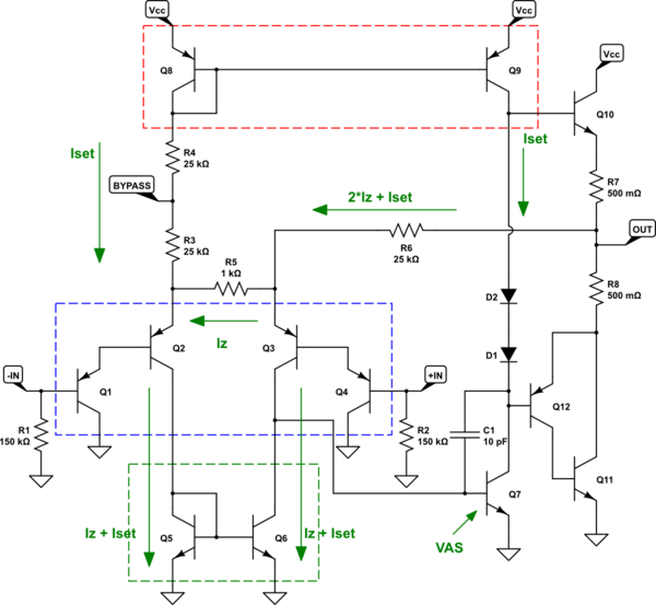
Also, note that when there is no signal present that the OUT voltage will be the same as the BIASBYPASS voltage. (The voltage drop across \$R_6\$ will be the same as the voltage drop across \$R_3\$.) You might provide a bipolar power supply here, tying schematic ground to the negative supply rail, \$V_{CC}\$ to the positive supply rail. and BIAS to supply ground (not the schematic ground.) In this case, the output will be roughly centered and will swing plus and minus around the supply ground.

schematic

simulate this circuit – Schematic created using CircuitLab

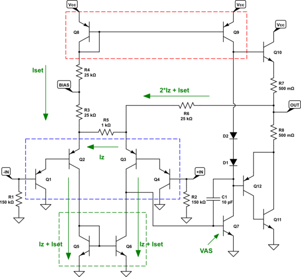
Also, note that when there is no signal present that the OUT voltage will be the same as the BIAS voltage. (The voltage drop across \$R_6\$ will be the same as the voltage drop across \$R_3\$.) You might provide a bipolar power supply here, tying schematic ground to the negative supply rail, \$V_{CC}\$ to the positive supply rail. and BIAS to supply ground (not the schematic ground.) In this case, the output will be roughly centered and will swing plus and minus around the supply ground.

schematic

simulate this circuit – Schematic created using CircuitLab

Also, note that when there is no signal present that the OUT voltage will be the same as the BYPASS voltage. (The voltage drop across \$R_6\$ will be the same as the voltage drop across \$R_3\$.)

better use of words
Source Link
jonk
  • 78.7k
  • 6
  • 81
  • 195

Also, note that when there is no signal present that the OUT voltage will be the same as the BIAS voltage. (The voltage drop across \$R_6\$ will be the same as the voltage drop across \$R_3\$.) If you providedYou might provide a bipolar power supply here, you tietying schematic ground to the negative supply rail, tie \$V_{CC}\$ to the positive supply rail,. and tie BIAS to supply ground (not the schematic ground.) In this case, the output will be roughly centered and will swing plus and minus around the supply ground.

Also, note that when there is no signal present that the OUT voltage will be the same as the BIAS voltage. (The voltage drop across \$R_6\$ will be the same as the voltage drop across \$R_3\$.) If you provided a bipolar power supply here, you tie schematic ground to the negative supply rail, tie \$V_{CC}\$ to the positive supply rail, and tie BIAS to ground. In this case, the output will be roughly centered and will swing plus and minus around ground.

Also, note that when there is no signal present that the OUT voltage will be the same as the BIAS voltage. (The voltage drop across \$R_6\$ will be the same as the voltage drop across \$R_3\$.) You might provide a bipolar power supply here, tying schematic ground to the negative supply rail, \$V_{CC}\$ to the positive supply rail. and BIAS to supply ground (not the schematic ground.) In this case, the output will be roughly centered and will swing plus and minus around the supply ground.

added 459 characters in body; added 67 characters in body
Source Link
jonk
  • 78.7k
  • 6
  • 81
  • 195

schematicschematic

simulate this circuitsimulate this circuit – Schematic created using CircuitLab

The two diodes place the output stage (\$Q_{10}\$, \$Q_{11}\$, and \$Q_{12}\$) into class-AB mode (hopefully), providing enough \$V_{BE}\$ separation for the output BJTs to maintain some modest, but likely low quiescent current. \$C_1\$ is just a miller compensation capacitor for the voltage amplifier stage (VAS) of \$Q_7\$. It's pretty small in order to provide a high slew rate, I suspect. \$Q_9\$ provides a stream of current of about \$I_{SET}\$ in magnitude, which is tapped into and used by the bases of the output stage BJTs. But \$Q_7\$ should typically be sinking the hog's share in a well-designed arrangement.

Also, note that when there is no signal present that the OUT voltage will be the same as the BIAS voltage. (The voltage drop across \$R_6\$ will be the same as the voltage drop across \$R_3\$.) If you provided a bipolar power supply here, you tie schematic ground to the negative supply rail, tie \$V_{CC}\$ to the positive supply rail, and tie BIAS to ground. In this case, the output will be roughly centered and will swing plus and minus around ground.

schematic

simulate this circuit – Schematic created using CircuitLab

The two diodes place the output stage (\$Q_{10}\$, \$Q_{11}\$, and \$Q_{12}\$) into class-AB mode (hopefully), providing enough \$V_{BE}\$ separation for the output BJTs to maintain some modest, but likely low quiescent current. \$C_1\$ is just a miller compensation capacitor for the voltage amplifier stage (VAS) of \$Q_7\$. \$Q_9\$ provides a stream of current of about \$I_{SET}\$ in magnitude, which is tapped into and used by the bases of the output stage BJTs. But \$Q_7\$ should typically be sinking the hog's share in a well-designed arrangement.

schematic

simulate this circuit – Schematic created using CircuitLab

The two diodes place the output stage (\$Q_{10}\$, \$Q_{11}\$, and \$Q_{12}\$) into class-AB mode (hopefully), providing enough \$V_{BE}\$ separation for the output BJTs to maintain some modest, but likely low quiescent current. \$C_1\$ is just a miller compensation capacitor for the voltage amplifier stage (VAS) of \$Q_7\$. It's pretty small in order to provide a high slew rate, I suspect. \$Q_9\$ provides a stream of current of about \$I_{SET}\$ in magnitude, which is tapped into and used by the bases of the output stage BJTs. But \$Q_7\$ should typically be sinking the hog's share in a well-designed arrangement.

Also, note that when there is no signal present that the OUT voltage will be the same as the BIAS voltage. (The voltage drop across \$R_6\$ will be the same as the voltage drop across \$R_3\$.) If you provided a bipolar power supply here, you tie schematic ground to the negative supply rail, tie \$V_{CC}\$ to the positive supply rail, and tie BIAS to ground. In this case, the output will be roughly centered and will swing plus and minus around ground.

updated schematic with currents
Source Link
jonk
  • 78.7k
  • 6
  • 81
  • 195
Loading
Source Link
jonk
  • 78.7k
  • 6
  • 81
  • 195
Loading