added 427 characters in body; added 11 characters in body; added 12 characters in body
Source Link
AaronD
  • 5.8k
  • 12
  • 38

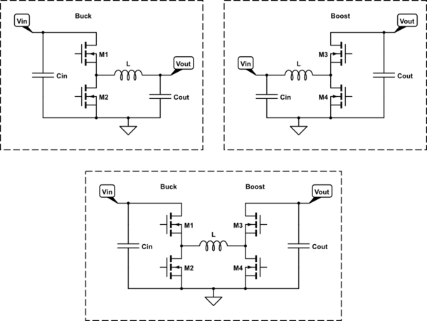
ThreePhaseEel has the correct answer, as already noted, but I'd like to redraw the schematic for my own understanding and to highlight the important parts. Maybe it'll help someone else too.
schematic

simulate this circuit – Schematic created using CircuitLab

So a Four-Switch Buck-Boost really is one followed by the other, at least as drawn in TPE's example. The rest of the components are for current and voltage feedback in various places or to adjust the controller's logic.

To simplify the control at the expense of some efficiency, M2 and M3 could be replaced with diodes. (both "pointing up") These are actually included parasitically in all the FETs (M1-M4), meaning that a manufacturer can't get rid of them even if they wanted to, so every symbol like that should be imagined with an "ordinary" silicon PN diode across it. The app note puts a couple of schottky diodes there anyway because their lower voltage drop results in less power loss if they ever were to conduct. (but still not nearly as good as their respective FETs being on)

ThreePhaseEel has the correct answer, as already noted, but I'd like to redraw the schematic for my own understanding and to highlight the important parts. Maybe it'll help someone else too.

schematic

simulate this circuit – Schematic created using CircuitLab

So a Four-Switch Buck-Boost really is one followed by the other, at least as drawn in TPE's example. The rest of the components are for current and voltage feedback in various places or to adjust the controller's logic.

To simplify the control at the expense of some efficiency, M2 and M3 could be replaced with diodes. (both "pointing up")

ThreePhaseEel has the correct answer, as already noted, but I'd like to redraw the schematic for my own understanding and to highlight the important parts. Maybe it'll help someone else too.

schematic

simulate this circuit – Schematic created using CircuitLab

So a Four-Switch Buck-Boost really is one followed by the other, at least as drawn in TPE's example. The rest of the components are for current and voltage feedback in various places or to adjust the controller's logic.

To simplify the control at the expense of some efficiency, M2 and M3 could be replaced with diodes. (both "pointing up") These are actually included parasitically in all the FETs (M1-M4), meaning that a manufacturer can't get rid of them even if they wanted to, so every symbol like that should be imagined with an "ordinary" silicon PN diode across it. The app note puts a couple of schottky diodes there anyway because their lower voltage drop results in less power loss if they ever were to conduct. (but still not nearly as good as their respective FETs being on)

Source Link
AaronD
  • 5.8k
  • 12
  • 38

ThreePhaseEel has the correct answer, as already noted, but I'd like to redraw the schematic for my own understanding and to highlight the important parts. Maybe it'll help someone else too.

schematic

simulate this circuit – Schematic created using CircuitLab

So a Four-Switch Buck-Boost really is one followed by the other, at least as drawn in TPE's example. The rest of the components are for current and voltage feedback in various places or to adjust the controller's logic.

To simplify the control at the expense of some efficiency, M2 and M3 could be replaced with diodes. (both "pointing up")