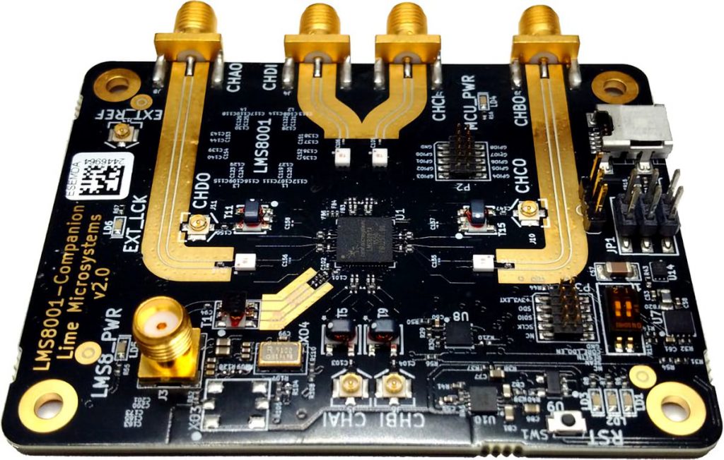
In the answers to my previous question "RF Design Basics", there is an explanationare explanations about the purpose of a golden ring around the PCB edge and around some parts (functional blocks) within the PCB.
However, I want to know what: What is the purpose of the golden area surrounding the RF traces, like in the Lime Microsystems board below.? I suppose it is, again, used as a shield, but does it have to be golden in this case when it is not intended for shell mounting ? Will the masked (painted) copper with the proper via stitching around do the same thing ? And, is there some rule that defines the width of the surrounding area that have to be golden ?
Thank you much for your time,

