Commonmark migration
Source Link

A basic current mirror is shown below:

[![enter image description here][1]][1]enter image description here
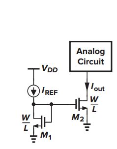
The load and reference current relationship is affected by channel length modulation: [![enter image description here][2]][2]enter image description here

In order to cancel the effects of channel length modulation, vds1 and vds2 need to be equal. A cascode current mirror is needed to make this happen, but how? The book I'm using is by Razavi.. [![enter image description here][3]][3]enter image description here
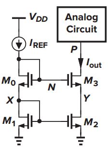
Vn = Vgs3 + Vds2

Then, in order to make Vds1=Vds2, vn must satisfy:

Vn = Vgs3 + Vds1 or Vn = Vgs3 + Vgs1

But from the circuit:

Vn=Vgs0 + Vgs1 !!!

How are Vgs0 and Vgs3 equal? [1]: https://i.sstatic.net/YmpuK.jpg [2]: https://i.sstatic.net/JMhXi.jpg [3]: https://i.sstatic.net/mZHs8.jpg

A basic current mirror is shown below:

[![enter image description here][1]][1]

The load and reference current relationship is affected by channel length modulation: [![enter image description here][2]][2]

In order to cancel the effects of channel length modulation, vds1 and vds2 need to be equal. A cascode current mirror is needed to make this happen, but how? The book I'm using is by Razavi.. [![enter image description here][3]][3]

Vn = Vgs3 + Vds2

Then, in order to make Vds1=Vds2, vn must satisfy:

Vn = Vgs3 + Vds1 or Vn = Vgs3 + Vgs1

But from the circuit:

Vn=Vgs0 + Vgs1 !!!

How are Vgs0 and Vgs3 equal? [1]: https://i.sstatic.net/YmpuK.jpg [2]: https://i.sstatic.net/JMhXi.jpg [3]: https://i.sstatic.net/mZHs8.jpg

A basic current mirror is shown below:

enter image description here

The load and reference current relationship is affected by channel length modulation: enter image description here

In order to cancel the effects of channel length modulation, vds1 and vds2 need to be equal. A cascode current mirror is needed to make this happen, but how? The book I'm using is by Razavi.. enter image description here

Vn = Vgs3 + Vds2

Then, in order to make Vds1=Vds2, vn must satisfy:

Vn = Vgs3 + Vds1 or Vn = Vgs3 + Vgs1

But from the circuit:

Vn=Vgs0 + Vgs1 !!!

How are Vgs0 and Vgs3 equal?

Source Link

How does a cascode current mirror maintain equal Vds of the bottom transistors?

A basic current mirror is shown below:

[![enter image description here][1]][1]

The load and reference current relationship is affected by channel length modulation: [![enter image description here][2]][2]

In order to cancel the effects of channel length modulation, vds1 and vds2 need to be equal. A cascode current mirror is needed to make this happen, but how? The book I'm using is by Razavi.. [![enter image description here][3]][3]

Vn = Vgs3 + Vds2

Then, in order to make Vds1=Vds2, vn must satisfy:

Vn = Vgs3 + Vds1 or Vn = Vgs3 + Vgs1

But from the circuit:

Vn=Vgs0 + Vgs1 !!!

How are Vgs0 and Vgs3 equal? [1]: https://i.sstatic.net/YmpuK.jpg [2]: https://i.sstatic.net/JMhXi.jpg [3]: https://i.sstatic.net/mZHs8.jpg