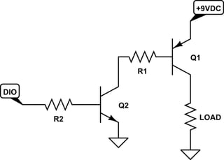
In addition to the answers you've already received, here is my suggestion.

simulate this circuit – Schematic created using CircuitLab
Resistor \$R_{LOAD}\$ is a "dummy" component; it is a placeholder for the actual circuit that you want to turn ON|OFF via Q1. To solve for the values of the "current limiting" resistors R1 and R2 proceed as follows.
- Determine the required current through the load, \$I_{LOAD}\$. For the purposes of this example assume \$I_{LOAD}=20\;mA\$. (n.b. I'm assuming the LOAD circuit has one or more components that limit the LOAD current to 20 mA when Q1 is ON.)
- For Q1 choose a PNP transistor whose rated collector current \$I_C\ge2I_{LOAD}\$. I'll choose for Q1 an ON Semiconductor 2N3906 PNP transistor whose \$I_C=200\;mA\$.
- Using Q1's data sheet determine the forward current gain when Q1 is operating in saturation mode (fully ON): \$\beta_{SAT}=10\$.
- Calculate Q1's base current when Q1 is operating in saturation mode: $$ Q1.I_{B(SAT)}=\frac{Q1.I_{C(SAT)}}{Q1.\beta_{SAT}}=\frac{20\;mA}{10}=2\;mA $$
- For Q2 chose an NPN transistor whose rated collector current \$I_C\ge 2\cdot Q1.I_{B(SAT)}\$. I'll chose an ON Semiconductor 2N3904 NPN transistor whose \$I_C=200\;mA\$.
- Using Q2's data sheet determine the forward current gain when Q2 is operating in saturation mode (fully ON): \$\beta_{SAT}=10\$.
- Calculate Q2's base current when Q2 is operating in saturation mode: $$ Q2.I_{B(SAT)}=\frac{Q2.I_{C(SAT)}}{Q2.\beta_{SAT}}=\frac{2\;mA}{10}=200\;\mu A $$
- Solve for R1. (n.b. Use the 2N3904 and 2N3906 data sheets to find values for \$V_{CE(SAT)}\$ and \$V_{BE(SAT)}\$.) (n.b. On a PNP transistor, current flows OUT of the transistor's base lead, and \$V_{BE(SAT)}=-V_{EB(SAT)}\$\$V_{BE(SAT)}\lt0\;V\$, and \$V_{EB(SAT)}=-V_{BE(SAT)}\$.) $$ R1=\frac{V_{R1}}{I_{R1}} \\=\frac{V_{CC}-Q1.V_{EB(sat)}-Q2.V_{CE(sat)}}{Q1.I_{B(sat)}} \\=\frac{9\;V-0.8\;V-0.05\;V}{2\;mA} \\=4.08\;k\Omega $$
- Choose R1's value as \$3.9\;k\Omega\pm5\;\%\$. (n.b. Calculate R1's power dissipation when Q2 is ON: \$P=I^2R\$. Choose for R1 a resistor whose power dissipation spec is >=2x its calculated power dissipation.)
- Solve for R2. (n.b. Use the microcontroller's data sheet to find \$V_{OH}\$ for the DIO pin. For example, assume we are using a Microchip Technology* ATmega328P *microcontroller and 5 V logic; see Chapter 30 "Electrical Specifications" in the data sheet. Use the 2N3904 data sheet to find \$V_{BE(SAT)}\$.) $$ R2=\frac{V_{R2}}{I_{R2}} \\=\frac{DIO.V_{OH}-Q2.V_{BE(sat)}}{Q2.I_{B(sat)}} \\=\frac{4.2\;V-0.7\;V}{200\;\mu A} \\=17.5\;k\Omega $$
- Choose R2's value as \$18\;k\Omega\pm5\;\%\$. (n.b. Calculate R2's power dissipation when Q2 is ON. Choose for R2 a resistor whose power dissipation spec is >=2x its calculated power dissipation.)
