added 201 characters in body
Source Link
Spehro 'speff' Pefhany
  • 422.3k
  • 23
  • 352
  • 949

This particular voltage regulator has no active clamping function so you're looking at some function of the output capacitance input voltage waveform and regulator characteristics.

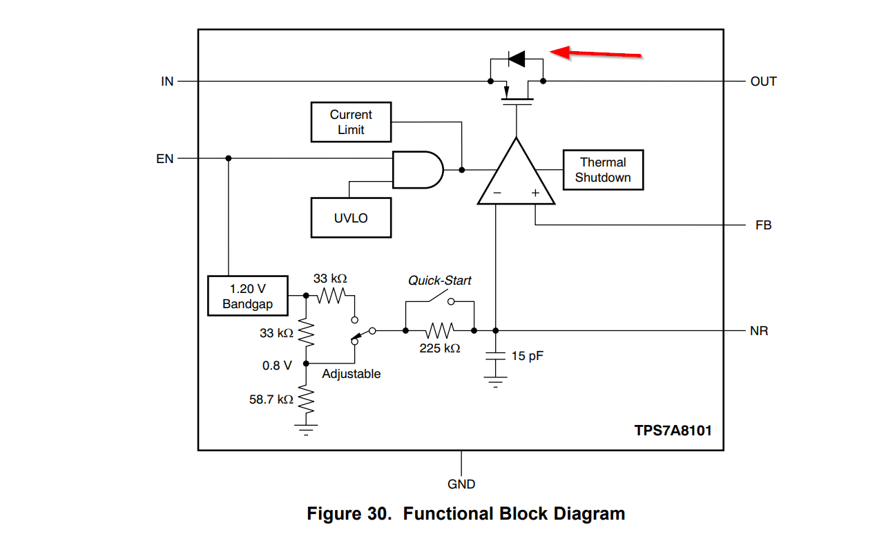
Case 1: If you actively pull the power input to the regulator down to 0V, the output capacitance will primarily discharge through the pass transistor body diode, at least down to 0.7V or so. See the block diagram below, which clearly shows a diode directly between output and input:

enter image description here

Case 2: If you open the input then the input capacitance and output capacitance will discharge through the bias network in the chip, perhaps via the body diode in part, and whatever load you've got on the output.

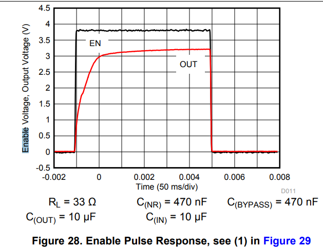
Case 3: If you disable the regulator through the enable input (with input power still applied) it will probably depend almost entirely upon the load current and output capacitance. The datasheet shows the typical output response to enable turning off, but it's with a rather low load resistance (33\$\Omega\$) so the RC time constant of the output capacitor and load is only 330usec which doesn't really show up at 50ms/div.

enter image description here

With the recommended feedback resistors and no other load, and with 10uF the time constant is more than 400ms so it could take more than 1 second to to drop down to << 1V.

If you need to have the regulator output drop down to some specific maximum voltage in a certain period of time under specific conditions, you can test a sample and add a large safety margin or buy a part that is specified for that kind of requirement.

For example, the LT3063 has an active discharge function that will take a 10uF output load capacitance down to < 10% of output voltage in 750us typical, 2ms maximum for enable controlled shutdown.

This particular voltage regulator has no active clamping function so you're looking at some function of the output capacitance input voltage waveform and regulator characteristics.

Case 1: If you actively pull the power input to the regulator down to 0V, the output capacitance will primarily discharge through the pass transistor body diode, at least down to 0.7V or so. See the block diagram below, which clearly shows a diode directly between output and input:

enter image description here

Case 2: If you open the input then the input capacitance and output capacitance will discharge through the bias network in the chip, perhaps via the body diode in part, and whatever load you've got on the output.

Case 3: If you disable the regulator through the enable input (with input power still applied) it will probably depend almost entirely upon the load current and output capacitance. The datasheet shows the typical output response to enable turning off, but it's with a rather low load resistance (33\$\Omega\$) so the RC time constant of the output capacitor and load is only 330usec which doesn't really show up at 50ms/div.

enter image description here

With the recommended feedback resistors and no other load, and with 10uF the time constant is more than 400ms so it could take more than 1 second to to drop down to << 1V.

If you need to have the regulator output drop down to some specific maximum voltage in a certain period of time under specific conditions, you can test a sample and add a large safety margin or buy a part that is specified for that kind of requirement.

For example, the LT3063 has an active discharge function that will take a 10uF output load capacitance down to < 10% of output voltage in 750us typical, 2ms maximum for enable controlled shutdown.
added 187 characters in body
Source Link
Spehro 'speff' Pefhany
  • 422.3k
  • 23
  • 352
  • 949

This particular voltage regulator has no active clamping function so you're looking at some function of the output capacitance input voltage waveform and regulator characteristics.

Case 1: If you actively pull the power input to the regulator down to 0V, the output capacitance will primarily discharge through the pass transistor body diode, at least down to 0.7V or so. See the block diagram below, which clearly shows a diode directly between output and input:

enter image description here

Case 2: If you open the input then the input capacitance and output capacitance will discharge through the bias network in the chip, perhaps via the body diode in part, and whatever load you've got on the output.

Case 3: If you disable the regulator through the enable input (with input power still applied) it will probably depend almost entirely upon the load current and output capacitance. The datasheet shows the typical output response to enable turning off, but it's with a rather low load resistance (33\$\Omega\$) so the RC time constant of the output capacitor and load is only 330usec which doesn't really show up at 50ms/div.

enter image description here

With the recommended feedback resistors and no other load, and with 10uF the time constant is more than 400ms so it could take more than 1 second to to drop down to << 1V.

If you need to have the regulator output drop down to some specific maximum voltage in a certain period of time under specific conditions, you can test a sample and add a large safety margin or buy a part that is specified for that kind of requirement.

This particular voltage regulator has no active clamping function so you're looking at some function of the output capacitance input voltage waveform and regulator characteristics.

If you actively pull the input to the regulator down to 0V, the output capacitance will primarily discharge through the pass transistor body diode, at least down to 0.7V or so. If you open the input then the input capacitance and output capacitance will discharge through the bias network in the chip, perhaps via the body diode in part, and whatever load you've got on the output. If you disable the regulator through the enable input (with input power still applied) it will probably depend almost entirely upon the load current and output capacitance. The datasheet shows the typical output response to enable turning off, but it's with a rather low load resistance (33\$\Omega\$) so the RC time constant of the output capacitor and load is only 330usec which doesn't really show up at 50ms/div.

enter image description here

With the recommended feedback resistors and no other load, and with 10uF the time constant is more than 400ms so it could take more than 1 second to to drop down to << 1V.

If you need to have the regulator output drop down to some specific maximum voltage in a certain period of time under specific conditions, you can test a sample and add a large safety margin or buy a part that is specified for that kind of requirement.

This particular voltage regulator has no active clamping function so you're looking at some function of the output capacitance input voltage waveform and regulator characteristics.

Case 1: If you actively pull the power input to the regulator down to 0V, the output capacitance will primarily discharge through the pass transistor body diode, at least down to 0.7V or so. See the block diagram below, which clearly shows a diode directly between output and input:

enter image description here

Case 2: If you open the input then the input capacitance and output capacitance will discharge through the bias network in the chip, perhaps via the body diode in part, and whatever load you've got on the output.

Case 3: If you disable the regulator through the enable input (with input power still applied) it will probably depend almost entirely upon the load current and output capacitance. The datasheet shows the typical output response to enable turning off, but it's with a rather low load resistance (33\$\Omega\$) so the RC time constant of the output capacitor and load is only 330usec which doesn't really show up at 50ms/div.

enter image description here

With the recommended feedback resistors and no other load, and with 10uF the time constant is more than 400ms so it could take more than 1 second to to drop down to << 1V.

If you need to have the regulator output drop down to some specific maximum voltage in a certain period of time under specific conditions, you can test a sample and add a large safety margin or buy a part that is specified for that kind of requirement.

Source Link
Spehro 'speff' Pefhany
  • 422.3k
  • 23
  • 352
  • 949

This particular voltage regulator has no active clamping function so you're looking at some function of the output capacitance input voltage waveform and regulator characteristics.

If you actively pull the input to the regulator down to 0V, the output capacitance will primarily discharge through the pass transistor body diode, at least down to 0.7V or so. If you open the input then the input capacitance and output capacitance will discharge through the bias network in the chip, perhaps via the body diode in part, and whatever load you've got on the output. If you disable the regulator through the enable input (with input power still applied) it will probably depend almost entirely upon the load current and output capacitance. The datasheet shows the typical output response to enable turning off, but it's with a rather low load resistance (33\$\Omega\$) so the RC time constant of the output capacitor and load is only 330usec which doesn't really show up at 50ms/div.

enter image description here

With the recommended feedback resistors and no other load, and with 10uF the time constant is more than 400ms so it could take more than 1 second to to drop down to << 1V.

If you need to have the regulator output drop down to some specific maximum voltage in a certain period of time under specific conditions, you can test a sample and add a large safety margin or buy a part that is specified for that kind of requirement.