fix typo
Source Link
Michael
  • 195
  • 8

A bodge solution that I am proceeding with for now is as follows: Raise the ground node of the timer circuit using a diode on the negative supply connection. Now the Vsat for the darlington output of U2 corresponds to an acceptable VIL at the ENABLE pin of 555 U3.

enter image description here

This is a temporary solution, giving the desired behaviour for now. Clearly, both the output and input circuits should be improved.

  • Since U2 does not need to pass significant current, re-selecting a "standard" BJT-optocoupler, with smaller Vsat; or a FET-optocoupler would improve the output envelope.
  • Large differences between the active regions of timer U3 and MOSFET Q2 mean they should switch from a preconditioned signal.

I'm aware that the full load-current flows through the added diode - this is no concern since the loads are small.

This bodge was a pretty convenient one to implement - an unused pin on my PCB header is adjacent to the GNDPWR pin, so I soldered the diode between these pins and moved the GNDPWR wire in the connector to suit.

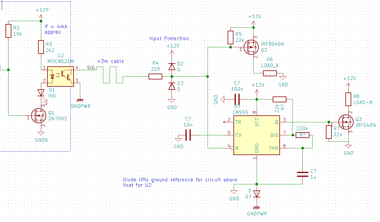
A bodge solution that I am proceeding with for now is as follows: Raise the ground node of the timer circuit using a diode on the negative supply connection. Now the Vsat for the darlington output of U2 corresponds to an acceptable VIL at the ENABLE pin of 555 U3.

enter image description here

This is a temporary solution, giving the desired behaviour for now. Clearly, both the output and input circuits should be improved.

  • Since U2 does not need to pass significant current, re-selecting a "standard" BJT-optocoupler, with smaller Vsat; or a FET-optocoupler would improve the output envelope.
  • Large differences between the active regions of timer U3 and MOSFET Q2 mean they should switch from a preconditioned signal.

I'm aware that the full load-current flows through the added diode - this is no concern since the loads are small.

This bodge was a pretty convenient one to implement - an unused pin on my PCB header is adjacent to the GNDPWR pin, so I soldered the diode between these pins and moved the GNDPWR the connector to suit.

A bodge solution that I am proceeding with for now is as follows: Raise the ground node of the timer circuit using a diode on the negative supply connection. Now the Vsat for the darlington output of U2 corresponds to an acceptable VIL at the ENABLE pin of 555 U3.

enter image description here

This is a temporary solution, giving the desired behaviour for now. Clearly, both the output and input circuits should be improved.

  • Since U2 does not need to pass significant current, re-selecting a "standard" BJT-optocoupler, with smaller Vsat; or a FET-optocoupler would improve the output envelope.
  • Large differences between the active regions of timer U3 and MOSFET Q2 mean they should switch from a preconditioned signal.

I'm aware that the full load-current flows through the added diode - this is no concern since the loads are small.

This bodge was a pretty convenient one to implement - an unused pin on my PCB header is adjacent to the GNDPWR pin, so I soldered the diode between these pins and moved the GNDPWR wire in the connector to suit.

add conclusion
Source Link
Michael
  • 195
  • 8

A bodge solution that I am proceeding with for now is as follows: Raise the ground node of the timer circuit using a diode on the negative supply connection. Now the Vsat for the darlington output of U2 corresponds to an acceptable VIL at the ENABLE pin of 555 U3.

enter image description here

This is a temporary solution, giving the desired behaviour for now. Clearly, both the output and input circuits should be improved.

  • Since U2 does not need to pass significant current, re-selecting a "standard" BJT-optocoupler, with smaller Vsat; or a FET-optocoupler would improve the output envelope.
  • Large differences between the active regions of timer U3 and MOSFET Q2 mean they should switch from a preconditioned signal.

I'm aware that the full load-current flows through the added diode - this is no concern since the loads are <50mA each; as it turns outsmall.

This bodge was a pretty convenient one to implement - an unused pin on my PCB header is adjacent to the GNDPWR pin, so I soldered the high power MOSFETS were needlessly overspecceddiode between these pins and moved the GNDPWR the connector to suit.

A bodge solution that I am proceeding with for now is as follows: Raise the ground node of the timer circuit using a diode on the negative supply connection. Now the Vsat for the darlington output of U2 corresponds to an acceptable VIL at the ENABLE pin of 555 U3.

enter image description here

This is a temporary solution, giving the desired behaviour for now. Clearly, both the output and input circuits should be improved.

  • Since U2 does not need to pass significant current, re-selecting a "standard" BJT-optocoupler, with smaller Vsat; or a FET-optocoupler would improve the output envelope.
  • Large differences between the active regions of timer U3 and MOSFET Q2 mean they should switch from a preconditioned signal.

I'm aware that the full load-current flows through the added diode - this is no concern since the loads are <50mA each; as it turns out, the high power MOSFETS were needlessly overspecced.

A bodge solution that I am proceeding with for now is as follows: Raise the ground node of the timer circuit using a diode on the negative supply connection. Now the Vsat for the darlington output of U2 corresponds to an acceptable VIL at the ENABLE pin of 555 U3.

enter image description here

This is a temporary solution, giving the desired behaviour for now. Clearly, both the output and input circuits should be improved.

  • Since U2 does not need to pass significant current, re-selecting a "standard" BJT-optocoupler, with smaller Vsat; or a FET-optocoupler would improve the output envelope.
  • Large differences between the active regions of timer U3 and MOSFET Q2 mean they should switch from a preconditioned signal.

I'm aware that the full load-current flows through the added diode - this is no concern since the loads are small.

This bodge was a pretty convenient one to implement - an unused pin on my PCB header is adjacent to the GNDPWR pin, so I soldered the diode between these pins and moved the GNDPWR the connector to suit.

Source Link
Michael
  • 195
  • 8

A bodge solution that I am proceeding with for now is as follows: Raise the ground node of the timer circuit using a diode on the negative supply connection. Now the Vsat for the darlington output of U2 corresponds to an acceptable VIL at the ENABLE pin of 555 U3.

enter image description here

This is a temporary solution, giving the desired behaviour for now. Clearly, both the output and input circuits should be improved.

  • Since U2 does not need to pass significant current, re-selecting a "standard" BJT-optocoupler, with smaller Vsat; or a FET-optocoupler would improve the output envelope.
  • Large differences between the active regions of timer U3 and MOSFET Q2 mean they should switch from a preconditioned signal.

I'm aware that the full load-current flows through the added diode - this is no concern since the loads are <50mA each; as it turns out, the high power MOSFETS were needlessly overspecced.