Commonmark migration
Source Link

I have a bottom gate TFT transistor:

  • W/l=320um
  • Substrate: corning glass
  • Gate: 60nm Molibdenum
  • Dielectric: 350 nm Ta2O5
  • Semiconductor: 30nm IGZO
  • S-D: Molibdenum 60nm

It is wired like in current mirror setup https://en.wikipedia.org/wiki/Current_mirror#Basic_MOSFET_current_mirror :
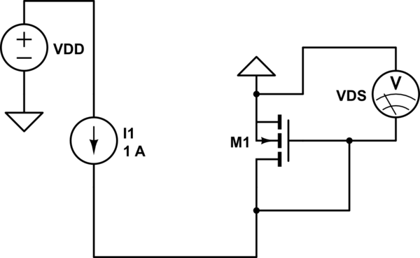
schematic

simulate this circuit – Schematic created using CircuitLab

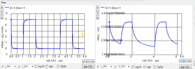
I am forcing pulses of current IDS and registering VGS=VDS This is what it looks like on the SMU:

  • Plot 1: CH1 IDS VS time
  • Plot 2: Ch1 VGS vs time

Plots

I want to wire a second transistor in the same way, get a recording VGS2 and then find the difference VGS1-VGS2.

The application

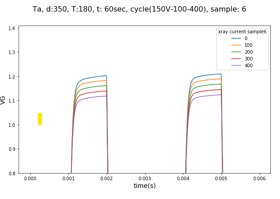
I am using the TFT to detect ionizing radiation: The X-ray radiation creates electron-hole pairs in the dielectric, which then affects the VGS recorded for a fixed ISD

Here is a plot showing how the VGS curve changes with the radiation exposure:

VGS vs Time

EDIT-from remices2 answer

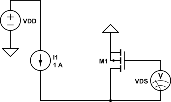
##EDIT-from remices2 answer## DoesDoes the circuit in the answer of remicles2 work? Since it has only gotten down votes for now, but I think because it wasn't using my original circuit (which I edited now since I think it was my circuit that was wrong.)

I have a bottom gate TFT transistor:

  • W/l=320um
  • Substrate: corning glass
  • Gate: 60nm Molibdenum
  • Dielectric: 350 nm Ta2O5
  • Semiconductor: 30nm IGZO
  • S-D: Molibdenum 60nm

It is wired like in current mirror setup https://en.wikipedia.org/wiki/Current_mirror#Basic_MOSFET_current_mirror :

schematic

simulate this circuit – Schematic created using CircuitLab

I am forcing pulses of current IDS and registering VGS=VDS This is what it looks like on the SMU:

  • Plot 1: CH1 IDS VS time
  • Plot 2: Ch1 VGS vs time

Plots

I want to wire a second transistor in the same way, get a recording VGS2 and then find the difference VGS1-VGS2.

The application

I am using the TFT to detect ionizing radiation: The X-ray radiation creates electron-hole pairs in the dielectric, which then affects the VGS recorded for a fixed ISD

Here is a plot showing how the VGS curve changes with the radiation exposure:

VGS vs Time

##EDIT-from remices2 answer## Does the circuit in the answer of remicles2 work? Since it has only gotten down votes for now, but I think because it wasn't using my original circuit (which I edited now since I think it was my circuit that was wrong.)
I have a bottom gate TFT transistor:

  • W/l=320um
  • Substrate: corning glass
  • Gate: 60nm Molibdenum
  • Dielectric: 350 nm Ta2O5
  • Semiconductor: 30nm IGZO
  • S-D: Molibdenum 60nm

It is wired like in current mirror setup https://en.wikipedia.org/wiki/Current_mirror#Basic_MOSFET_current_mirror :

schematic

simulate this circuit – Schematic created using CircuitLab

I am forcing pulses of current IDS and registering VGS=VDS This is what it looks like on the SMU:

  • Plot 1: CH1 IDS VS time
  • Plot 2: Ch1 VGS vs time

Plots

I want to wire a second transistor in the same way, get a recording VGS2 and then find the difference VGS1-VGS2.

The application

I am using the TFT to detect ionizing radiation: The X-ray radiation creates electron-hole pairs in the dielectric, which then affects the VGS recorded for a fixed ISD

Here is a plot showing how the VGS curve changes with the radiation exposure:

VGS vs Time

EDIT-from remices2 answer

Does the circuit in the answer of remicles2 work? Since it has only gotten down votes for now, but I think because it wasn't using my original circuit (which I edited now since I think it was my circuit that was wrong.)
added 4 characters in body
Source Link
JRE
  • 73.5k
  • 10
  • 112
  • 194

Amplyfy Amplify voltage between Transistorstransistors in Currenta current mirror setup?

I have a Bottom Gatebottom gate TFT transistor:

  • W/l=320um
  • Substrate: corning glass
  • Gate: 60nm Molibdenum
  • Dielectric: 350 nm Ta2O5
  • Semiconductor: 30nm IGZO
  • S-D: Molibdenum 60nm

It is wired like in current mirror setup https://en.wikipedia.org/wiki/Current_mirror#Basic_MOSFET_current_mirror :

schematic

simulate this circuit – Schematic created using CircuitLab

I am forcing pulses of Currentcurrent IDS and registering VGS=VDS This is what it looks like on the SMU:

  • PLotPlot 1: CH1 IDS VS time
  • Plot 2: Ch1 VGS vs time

Plots

I want to wire a second transistor in the same way, get a recording VGS2 and then find the difference VGS1-VGS2.

The application

I am using the TFT to detect Ionizingionizing radiation: The X-ray radiation creates electron-hole pairs in the Dielectricdielectric, which then affectaffects the VGS recorded for a fixed ISD

Here is a plot showing how the VGS curve changes with the radiation exposure  :

VGS vs Time

##EDIT-from remices2 answer## Does the circuit in the answer of remicles2 work? sinceSince it has only gotten down votes for now, but I think because it wasn't using my original circuit (which I edited now since I think it was my circuit that was wrong.)

Amplyfy voltage between Transistors in Current mirror setup?

I have a Bottom Gate TFT transistor:

  • W/l=320um
  • Substrate: corning glass
  • Gate: 60nm Molibdenum
  • Dielectric: 350 nm Ta2O5
  • Semiconductor: 30nm IGZO
  • S-D: Molibdenum 60nm

It is wired like in current mirror setup https://en.wikipedia.org/wiki/Current_mirror#Basic_MOSFET_current_mirror :

schematic

simulate this circuit – Schematic created using CircuitLab

I am forcing pulses of Current IDS and registering VGS=VDS This is what it looks like on the SMU:

  • PLot 1: CH1 IDS VS time
  • Plot 2: Ch1 VGS vs time

Plots

I want to wire a second transistor in the same way, get a recording VGS2 and then find the difference VGS1-VGS2.

The application

I am using the TFT to detect Ionizing radiation: The X-ray radiation creates electron-hole pairs in the Dielectric, which then affect the VGS recorded for a fixed ISD

Here is a plot showing how the VGS curve changes with the radiation exposure  VGS vs Time

##EDIT-from remices2 answer## Does the circuit in the answer of remicles2 work? since it has only gotten down votes for now, but I think because it wasn't using my original circuit (which I edited now since I think it was my circuit that was wrong)

Amplify voltage between transistors in a current mirror setup?

I have a bottom gate TFT transistor:

  • W/l=320um
  • Substrate: corning glass
  • Gate: 60nm Molibdenum
  • Dielectric: 350 nm Ta2O5
  • Semiconductor: 30nm IGZO
  • S-D: Molibdenum 60nm

It is wired like in current mirror setup https://en.wikipedia.org/wiki/Current_mirror#Basic_MOSFET_current_mirror :

schematic

simulate this circuit – Schematic created using CircuitLab

I am forcing pulses of current IDS and registering VGS=VDS This is what it looks like on the SMU:

  • Plot 1: CH1 IDS VS time
  • Plot 2: Ch1 VGS vs time

Plots

I want to wire a second transistor in the same way, get a recording VGS2 and then find the difference VGS1-VGS2.

The application

I am using the TFT to detect ionizing radiation: The X-ray radiation creates electron-hole pairs in the dielectric, which then affects the VGS recorded for a fixed ISD

Here is a plot showing how the VGS curve changes with the radiation exposure:

VGS vs Time

##EDIT-from remices2 answer## Does the circuit in the answer of remicles2 work? Since it has only gotten down votes for now, but I think because it wasn't using my original circuit (which I edited now since I think it was my circuit that was wrong.)

Changed TFT connection- connected Drain-gate
Source Link
Leo
  • 251
  • 1
  • 8

I have a Bottom Gate TFT transistor:

  • W/l=320um
  • Substrate: corning glass
  • Gate: 60nm Molibdenum
  • Dielectric: 350 nm Ta2O5
  • Semiconductor: 30nm IGZO
  • S-D: Molibdenum 60nm

It is wired like in current mirror setup https://en.wikipedia.org/wiki/Current_mirror#Basic_MOSFET_current_mirror :

schematicschematic

simulate this circuitsimulate this circuit – Schematic created using CircuitLab

I am forcing pulses of Current IDS and registering VGS=VDS This is what it looks like on the SMU:

  • PLot 1: CH1 IDS VS time
  • Plot 2: Ch1 VGS vs time

Plots

I want to wire a second transistor in the same way, get a recording VGS2 and then find the difference VGS1-VGS2.

The application

I am using the TFT to detect Ionizing radiation: The X-ray radiation creates electron-hole pairs in the Dielectric, which then affect the VGS recorded for a fixed ISD

Here is a plot showing how the VGS curve changes with the radiation exposure VGS vs Time

##EDIT-from remices2 answer## Does the circuit in the answer of remicles2 work? since it has only gotten down votes for now, but I think because it wasn't using my original circuit (which I edited now since I think it was my circuit that was wrong)

I have a Bottom Gate TFT transistor:

  • W/l=320um
  • Substrate: corning glass
  • Gate: 60nm Molibdenum
  • Dielectric: 350 nm Ta2O5
  • Semiconductor: 30nm IGZO
  • S-D: Molibdenum 60nm

It is wired like in current mirror setup https://en.wikipedia.org/wiki/Current_mirror#Basic_MOSFET_current_mirror :

schematic

simulate this circuit – Schematic created using CircuitLab

I am forcing pulses of Current IDS and registering VGS=VDS This is what it looks like on the SMU:

  • PLot 1: CH1 IDS VS time
  • Plot 2: Ch1 VGS vs time

Plots

I want to wire a second transistor in the same way, get a recording VGS2 and then find the difference VGS1-VGS2.

The application

I am using the TFT to detect Ionizing radiation: The X-ray radiation creates electron-hole pairs in the Dielectric, which then affect the VGS recorded for a fixed ISD

Here is a plot showing how the VGS curve changes with the radiation exposure VGS vs Time

##EDIT-from remices2 answer## Does the circuit in the answer of remicles2 work? since it has only gotten down votes for now, but I think because it wasn't using my original circuit (which I edited now since I think it was my circuit that was wrong)

Changed TFT connection- connected Drain-gate
Source Link
Leo
  • 251
  • 1
  • 8
Loading
Example result
Source Link
Leo
  • 251
  • 1
  • 8
Loading
Changed the symbol to TFT
Source Link
Leo
  • 251
  • 1
  • 8
Loading
added 153 characters in body
Source Link
Leo
  • 251
  • 1
  • 8
Loading
added 190 characters in body
Source Link
Leo
  • 251
  • 1
  • 8
Loading
All information
Source Link
Leo
  • 251
  • 1
  • 8
Loading
added 315 characters in body; edited title
Source Link
Leo
  • 251
  • 1
  • 8
Loading
edited title
Link
JRE
  • 73.5k
  • 10
  • 112
  • 194
Loading
added 7 characters in body; edited title
Source Link
JRE
  • 73.5k
  • 10
  • 112
  • 194
Loading
Source Link
Leo
  • 251
  • 1
  • 8
Loading