added 500 characters in body
Source Link
D.A.S.
  • 148k
  • 3
  • 56
  • 190

The minimum area of the chip is determined by the most cost effective solution not the smallest physical possible cut.

The smallest cut defect-free with a kerf is roughly equal to the wafer thickness and the slotted diamond saw roughly equal to 1/2 of the wafer thickness.

Thus the question should be what is the cheapest way to process single diode junctions. As the biggest demand for single diode junctions appears to be LED's , the question should be what is the maximum number of LED's per wafer? Economy has driven the size of the LED up. There is no benefit to going smaller.

For any given chip on a die and wafer size, this calculation limits the maximum number of Die Per Wafer.

This is not the limit but is a calculator to determine the mechanical yield of a wafer.

enter image description here

The trend now is to make small flip chips with bump pads stacked on a system in packagesystem in package (SiP) or system-in-a-package with a number of integrated circuits enclosed in a single chip carrier package.

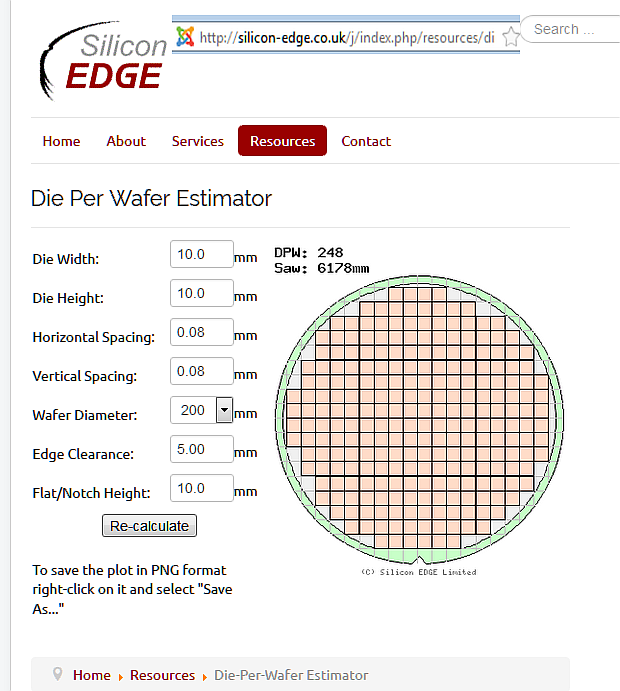
The minimum area of the chip is determined by the most cost effective solution not the smallest physical possible cut.

The smallest cut defect-free with a kerf is roughly equal to the wafer thickness and the slotted diamond saw roughly equal to 1/2 of the wafer thickness.

Thus the question should be what is the cheapest way to process single diode junctions. As the biggest demand for single diode junctions appears to be LED's , the question should be what is the maximum number of LED's per wafer? Economy has driven the size of the LED up. There is no benefit to going smaller.

For any given chip on a die and wafer size, this calculation limits the maximum number of Die Per Wafer.

This is not the limit but is a calculator to determine the mechanical yield of a wafer.

enter image description here

The trend now is to make small chips stacked on a system in package (SiP) or system-in-a-package with a number of integrated circuits enclosed in a single chip carrier package.

The minimum area of the chip is determined by the most cost effective solution not the smallest physical possible cut.

The smallest cut defect-free with a kerf is roughly equal to the wafer thickness and the slotted diamond saw roughly equal to 1/2 of the wafer thickness.

Thus the question should be what is the cheapest way to process single diode junctions. As the biggest demand for single diode junctions appears to be LED's , the question should be what is the maximum number of LED's per wafer? Economy has driven the size of the LED up. There is no benefit to going smaller.

For any given chip on a die and wafer size, this calculation limits the maximum number of Die Per Wafer.

This is not the limit but is a calculator to determine the mechanical yield of a wafer.

enter image description here

The trend now is to make small flip chips with bump pads stacked on a system in package (SiP) or system-in-a-package with a number of integrated circuits enclosed in a single chip carrier package.

added 500 characters in body
Source Link
D.A.S.
  • 148k
  • 3
  • 56
  • 190

The minimum area of the chip is determined by the wire bonding pad size and margins around itmost cost effective solution not the smallest physical possible cut.

The smallest cut defect-free with a kerf is roughly equal to the wafer thickness and the slotted diamond saw roughly equal to 1/2 of the wafer thickness. For

Thus the question should be what is the cheapest way to process single diode junctions. As the biggest demand for single diode junctions appears to be LED's , the question should be what is the maximum number of LED's per wafer? Economy has driven the size of the LED up. There is no benefit to going smaller.

For any given chip on a die and wafer size, this calculation limits the maximum number of Die Per Wafer.

This is not the limit but is a calculator to determine the mechanical yield of a wafer.

enter image description here

The trend now is to make small chips stacked on a system in package (SiP) or system-in-a-package with a number of integrated circuits enclosed in a single chip carrier package.

The minimum area of the chip is determined by the wire bonding pad size and margins around it cut with a diamond saw. For any given chip on a die and wafer size, this limits the maximum number of Die Per Wafer.

This is not the limit but is a calculator to determine the mechanical yield of a wafer.

enter image description here

The minimum area of the chip is determined by the most cost effective solution not the smallest physical possible cut.

The smallest cut defect-free with a kerf is roughly equal to the wafer thickness and the slotted diamond saw roughly equal to 1/2 of the wafer thickness.

Thus the question should be what is the cheapest way to process single diode junctions. As the biggest demand for single diode junctions appears to be LED's , the question should be what is the maximum number of LED's per wafer? Economy has driven the size of the LED up. There is no benefit to going smaller.

For any given chip on a die and wafer size, this calculation limits the maximum number of Die Per Wafer.

This is not the limit but is a calculator to determine the mechanical yield of a wafer.

enter image description here

The trend now is to make small chips stacked on a system in package (SiP) or system-in-a-package with a number of integrated circuits enclosed in a single chip carrier package.

Source Link
D.A.S.
  • 148k
  • 3
  • 56
  • 190

The minimum area of the chip is determined by the wire bonding pad size and margins around it cut with a diamond saw. For any given chip on a die and wafer size, this limits the maximum number of Die Per Wafer.

This is not the limit but is a calculator to determine the mechanical yield of a wafer.

enter image description here