Commonmark migration
Source Link

The NCS333 cannot operate well as a comparator at 2.5V with an insufficient swing to get the rated RdsOn. Thus at high RdsOn, and low loads the hysteresis reduces to the point where you have almost none.

Put a level shifter or inverter to get a full swing on the output and swap inputs or try more hysteresis.

You should at least pay more attention to the output swing specs on the Op Amp and Vgs vs RdsOn and use a better comparator instead of a precision Op Amp.

edit:

This is what concerned me about the gate drive voltage using this Op Amp as a low voltage comparator. p7 https://www.onsemi.com/pub/Collateral/NCS333-D.PDF

[![enter image description here][1]][1]enter image description here
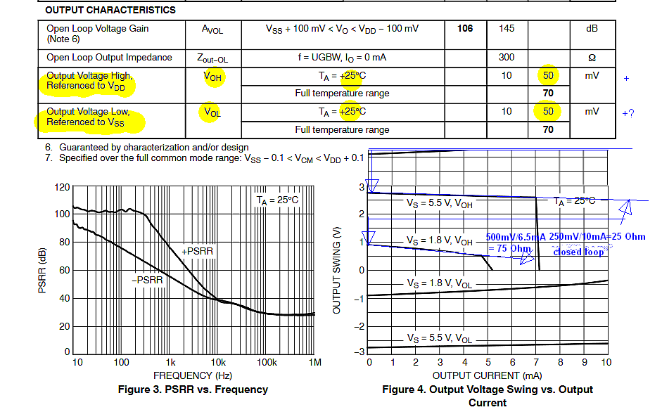
Adding a large gate resistor will help decouple reactance effects with positive feedback that you have being reduced by the output swing. The table implies a rail to rail CMOS swing output with 50mV rail offset, while the curves imply the output swing is far from Rail to Rail yet Vdd, Vss implied it is still CMOS.

After starting at it for a while, I saw the error in my interpretation now. Where the graph says Vs=5.5 meaning supply, they are using bipolar supplies here, but only define it as Vdd-Vss=Vs, so the graphs all start with a 50% swing.

Conclusion

My corrected analysis indicates you have excess gain at the resonant frequency due to 3rd order effects reducing phase margin and AC hysteresis with the load R load and C of supercap approaching the open-loop pole of the Op Amp., which may be corrected by suitable compensation.

There are 3rd order effects with RC capacitances in 3 parts (IC, FET-Ciss, Supercap) each add a pole and reducing load R pushes the pole up near the IC open-loop breakpoint.

Non-linear effects of IC: Hysteresis results in zero gain, yet the IC open loop has 130dB typ gain with a breakpoint well below 10Hz. With 10F and 1.1 Ohms, that's a bit higher.

Recommendations

The improve your stability, you can add phase-lead RC compensation or switch to a bipolar comparator or decouple the gate Ciss with a large series resistor to lower the gain at the resonant frequency with Ciss using say 10k ohm. [1]: https://i.sstatic.net/1FIal.png

The NCS333 cannot operate well as a comparator at 2.5V with an insufficient swing to get the rated RdsOn. Thus at high RdsOn, and low loads the hysteresis reduces to the point where you have almost none.

Put a level shifter or inverter to get a full swing on the output and swap inputs or try more hysteresis.

You should at least pay more attention to the output swing specs on the Op Amp and Vgs vs RdsOn and use a better comparator instead of a precision Op Amp.

edit:

This is what concerned me about the gate drive voltage using this Op Amp as a low voltage comparator. p7 https://www.onsemi.com/pub/Collateral/NCS333-D.PDF

[![enter image description here][1]][1]

Adding a large gate resistor will help decouple reactance effects with positive feedback that you have being reduced by the output swing. The table implies a rail to rail CMOS swing output with 50mV rail offset, while the curves imply the output swing is far from Rail to Rail yet Vdd, Vss implied it is still CMOS.

After starting at it for a while, I saw the error in my interpretation now. Where the graph says Vs=5.5 meaning supply, they are using bipolar supplies here, but only define it as Vdd-Vss=Vs, so the graphs all start with a 50% swing.

Conclusion

My corrected analysis indicates you have excess gain at the resonant frequency due to 3rd order effects reducing phase margin and AC hysteresis with the load R load and C of supercap approaching the open-loop pole of the Op Amp., which may be corrected by suitable compensation.

There are 3rd order effects with RC capacitances in 3 parts (IC, FET-Ciss, Supercap) each add a pole and reducing load R pushes the pole up near the IC open-loop breakpoint.

Non-linear effects of IC: Hysteresis results in zero gain, yet the IC open loop has 130dB typ gain with a breakpoint well below 10Hz. With 10F and 1.1 Ohms, that's a bit higher.

Recommendations

The improve your stability, you can add phase-lead RC compensation or switch to a bipolar comparator or decouple the gate Ciss with a large series resistor to lower the gain at the resonant frequency with Ciss using say 10k ohm. [1]: https://i.sstatic.net/1FIal.png

The NCS333 cannot operate well as a comparator at 2.5V with an insufficient swing to get the rated RdsOn. Thus at high RdsOn, and low loads the hysteresis reduces to the point where you have almost none.

Put a level shifter or inverter to get a full swing on the output and swap inputs or try more hysteresis.

You should at least pay more attention to the output swing specs on the Op Amp and Vgs vs RdsOn and use a better comparator instead of a precision Op Amp.

edit:

This is what concerned me about the gate drive voltage using this Op Amp as a low voltage comparator. p7 https://www.onsemi.com/pub/Collateral/NCS333-D.PDF

enter image description here

Adding a large gate resistor will help decouple reactance effects with positive feedback that you have being reduced by the output swing. The table implies a rail to rail CMOS swing output with 50mV rail offset, while the curves imply the output swing is far from Rail to Rail yet Vdd, Vss implied it is still CMOS.

After starting at it for a while, I saw the error in my interpretation now. Where the graph says Vs=5.5 meaning supply, they are using bipolar supplies here, but only define it as Vdd-Vss=Vs, so the graphs all start with a 50% swing.

Conclusion

My corrected analysis indicates you have excess gain at the resonant frequency due to 3rd order effects reducing phase margin and AC hysteresis with the load R load and C of supercap approaching the open-loop pole of the Op Amp., which may be corrected by suitable compensation.

There are 3rd order effects with RC capacitances in 3 parts (IC, FET-Ciss, Supercap) each add a pole and reducing load R pushes the pole up near the IC open-loop breakpoint.

Non-linear effects of IC: Hysteresis results in zero gain, yet the IC open loop has 130dB typ gain with a breakpoint well below 10Hz. With 10F and 1.1 Ohms, that's a bit higher.

Recommendations

The improve your stability, you can add phase-lead RC compensation or switch to a bipolar comparator or decouple the gate Ciss with a large series resistor to lower the gain at the resonant frequency with Ciss using say 10k ohm.

added 1726 characters in body
Source Link
D.A.S.
  • 148k
  • 3
  • 56
  • 190

The NCS333 cannot operate well as a comparator at 2.5V with an insufficient swing to get the rated RdsOn. Thus at high RdsOn, and low loads the hysteresis reduces to the point where you have almost none.

Put a level shifter or inverter to get a full swing on the output and swap inputs or try more hysteresis.

You should at least pay more attention to the output swing specs on the Op Amp and Vgs vs RdsOn and use a better comparator instead of a precision Op Amp.

edit:

This is what concerned me about the gate drive voltage using this Op Amp as a low voltage comparator. p7 https://www.onsemi.com/pub/Collateral/NCS333-D.PDF

[![enter image description here][1]][1]

Adding a large gate resistor will help decouple reactance effects with positive feedback that you have being reduced by the output swing. The table implies a rail to rail CMOS swing output with 50mV rail offset, while the curves imply the output swing is far from Rail to Rail yet Vdd, Vss implied it is still CMOS.

After starting at it for a while, I saw the error in my interpretation now. Where the graph says Vs=5.5 meaning supply, they are using bipolar supplies here, but only define it as Vdd-Vss=Vs, so the graphs all start with a 50% swing.

Conclusion

My corrected analysis indicates you have excess gain at the resonant frequency due to 3rd order effects reducing phase margin and AC hysteresis with the load R load and C of supercap approaching the open-loop pole of the Op Amp., which may be corrected by suitable compensation.

There are 3rd order effects with RC capacitances in 3 parts (IC, FET-Ciss, Supercap) each add a pole and reducing load R pushes the pole up near the IC open-loop breakpoint.

Non-linear effects of IC: Hysteresis results in zero gain, yet the IC open loop has 130dB typ gain with a breakpoint well below 10Hz. With 10F and 1.1 Ohms, that's a bit higher.

Recommendations

The improve your stability, you can add phase-lead RC compensation or switch to a bipolar comparator or decouple the gate Ciss with a large series resistor to lower the gain at the resonant frequency with Ciss using say 10k ohm. [1]: https://i.sstatic.net/1FIal.png

The NCS333 cannot operate well as a comparator at 2.5V with an insufficient swing to get the rated RdsOn. Thus at high RdsOn, and low loads the hysteresis reduces to the point where you have almost none.

Put a level shifter or inverter to get a full swing on the output and swap inputs or try more hysteresis.

You should at least pay more attention to the output swing specs on the Op Amp and Vgs vs RdsOn and use a better comparator instead of a precision Op Amp.

edit:

This is what concerned me about the gate drive voltage using this Op Amp as a low voltage comparator. p7 https://www.onsemi.com/pub/Collateral/NCS333-D.PDF

[![enter image description here][1]][1]

Adding a large gate resistor will help decouple reactance effects with positive feedback that you have being reduced by the output swing. The table implies a rail to rail CMOS swing output with 50mV rail offset, while the curves imply the output swing is far from Rail to Rail yet Vdd, Vss implied it is still CMOS.

After starting at it for a while, I saw the error in my interpretation now. Where the graph says Vs=5.5 meaning supply, they are using bipolar supplies here, but only define it as Vdd-Vss=Vs, so the graphs all start with a 50% swing.

Conclusion

My corrected analysis indicates you have excess gain at the resonant frequency due to 3rd order effects reducing phase margin and AC hysteresis with the load R load and C of supercap approaching the open-loop pole of the Op Amp., which may be corrected by suitable compensation.

There are 3rd order effects with RC capacitances in 3 parts (IC, FET-Ciss, Supercap) each add a pole and reducing load R pushes the pole up near the IC open-loop breakpoint.

Non-linear effects of IC: Hysteresis results in zero gain, yet the IC open loop has 130dB typ gain with a breakpoint well below 10Hz. With 10F and 1.1 Ohms, that's a bit higher.

Recommendations

The improve your stability, you can add phase-lead RC compensation or switch to a bipolar comparator or decouple the gate Ciss with a large series resistor to lower the gain at the resonant frequency with Ciss using say 10k ohm. [1]: https://i.sstatic.net/1FIal.png

Source Link
D.A.S.
  • 148k
  • 3
  • 56
  • 190

The NCS333 cannot operate well as a comparator at 2.5V with an insufficient swing to get the rated RdsOn. Thus at high RdsOn, and low loads the hysteresis reduces to the point where you have almost none.

Put a level shifter or inverter to get a full swing on the output and swap inputs or try more hysteresis.

You should at least pay more attention to the output swing specs on the Op Amp and Vgs vs RdsOn and use a better comparator instead of a precision Op Amp.