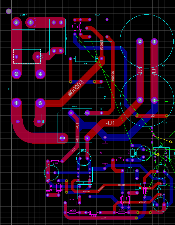
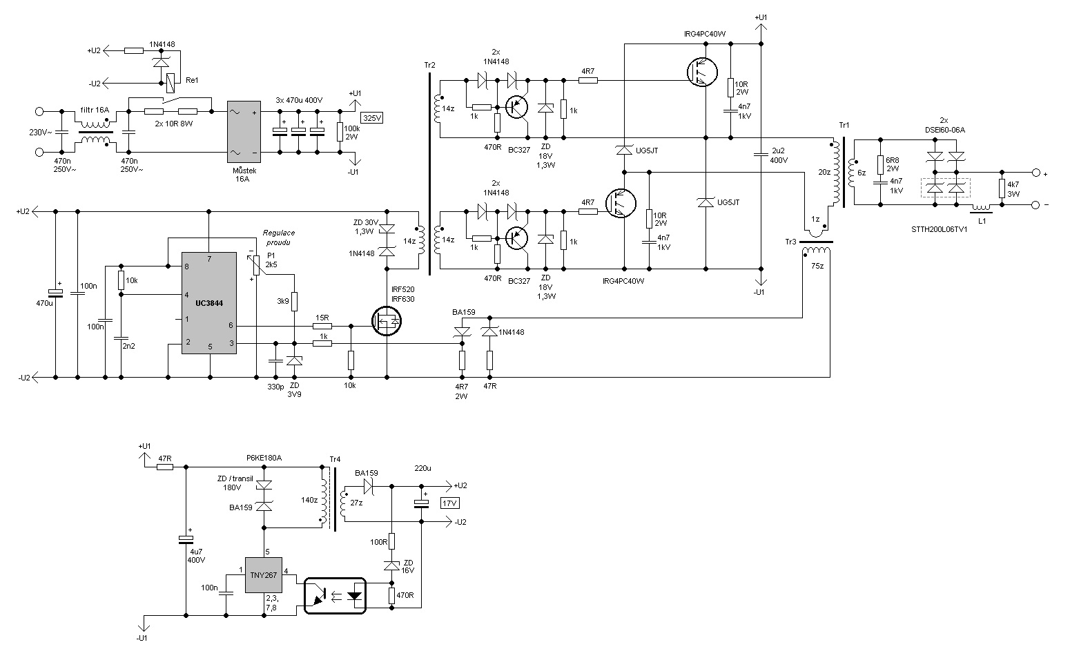
My attempt at drawing the PCB:

The routes are drawn on both layers and the thickness of the power route is 600 mil(300 on top and 300 on bottom). It is necessary to support ~15A. The question is, how do I make the current pass from the top to the bottom if the component pads are small or very small? Can I put vias near the pad, and how? Is it necessary to add vias next to each component? :) Is parasitic capacity formed between the same routes if they are on the top and bottom, or is ok? Is the voltage the same on the Top and Bottom on the same route? What rules should I take into account in this case? (any answer is helpful, thx)

