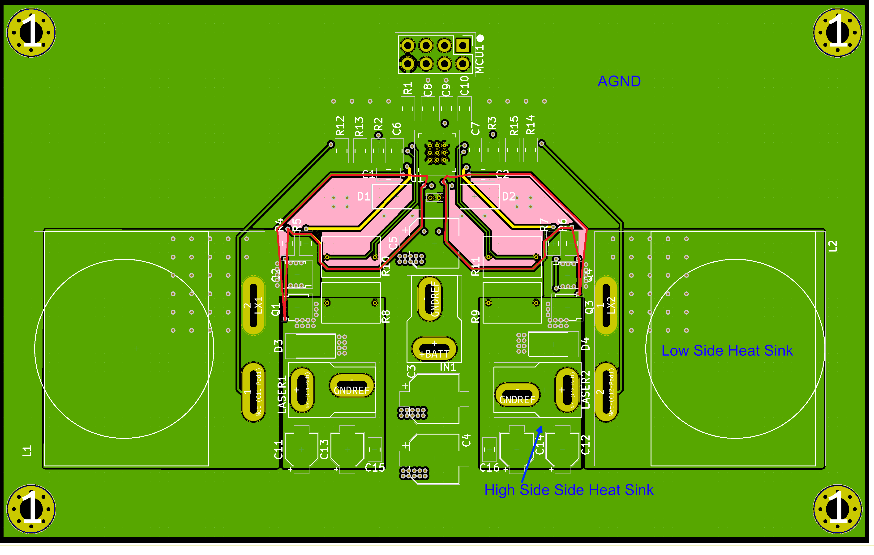
The high-side gate drive loop is bigger than it needs to be. The high-side gate drive signal is floating so it doesn't use the ground as its return path. Since it is the bootstrap capacitor which is powering that loop, the current flows using the common node between half-bridge capacitorsMOSFETs for its return path back to the bootstrap capacitor.
The current flows from through C1 into pin 2, out of the IC through pin 3, through the gate-source of Q1, and back to the IC through pin 1. Something similar happens for Q3.
This forms two massive loops on Layer 2 (outlined in red). The loop area is in pink and even with minimal changes to your current layout you could move the traces at the top of the loop down to completely get rid of the pink parallelograms. This would immediately halve your loop area but the loop is still really big but you can't get it any smaller with this layout since the low-side gate drive trace (outlined in yellow) is sitting in between the high-side gate drive trace and its return trace.
You made the high and low side gate drive traces (coming from pins 3/6 and 32/9, respectively) dance around each other on layer 2 near the IC so they would not block each other getting to the gate resistors. This resulted in the low-side gate drive traces coming from pins 32 and 9 get in between the high-side gate drive trace (pins 3/6) and its return trace (pins 1/8), preventing you from tightening up the high-side gate drive loop.
The natural pin ordering should have prevented this from happening but your dancing got around it. But you don't need to do this if sending one of the traces on a different layer. It looks like you can send the high-side gate signal (pins 3 and 6) through layer 4 without interrupting any plane currents and making them take detours around the traces). This would let you get the gate drive traces (pins 3 and 6) right under its return trace (pins 1 and 8). Do that if you can.
Then rejig the lowisde gate drive trace (outlined in yellow, pins 32 and 9) to be shorter and more direct.

