deleted 7 characters in body
Source Link
adlib33e
  • 47
  • 2
  • 9

Looking for suggestions as to designing the ground layer of a PCB.

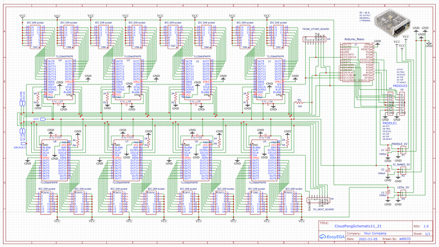
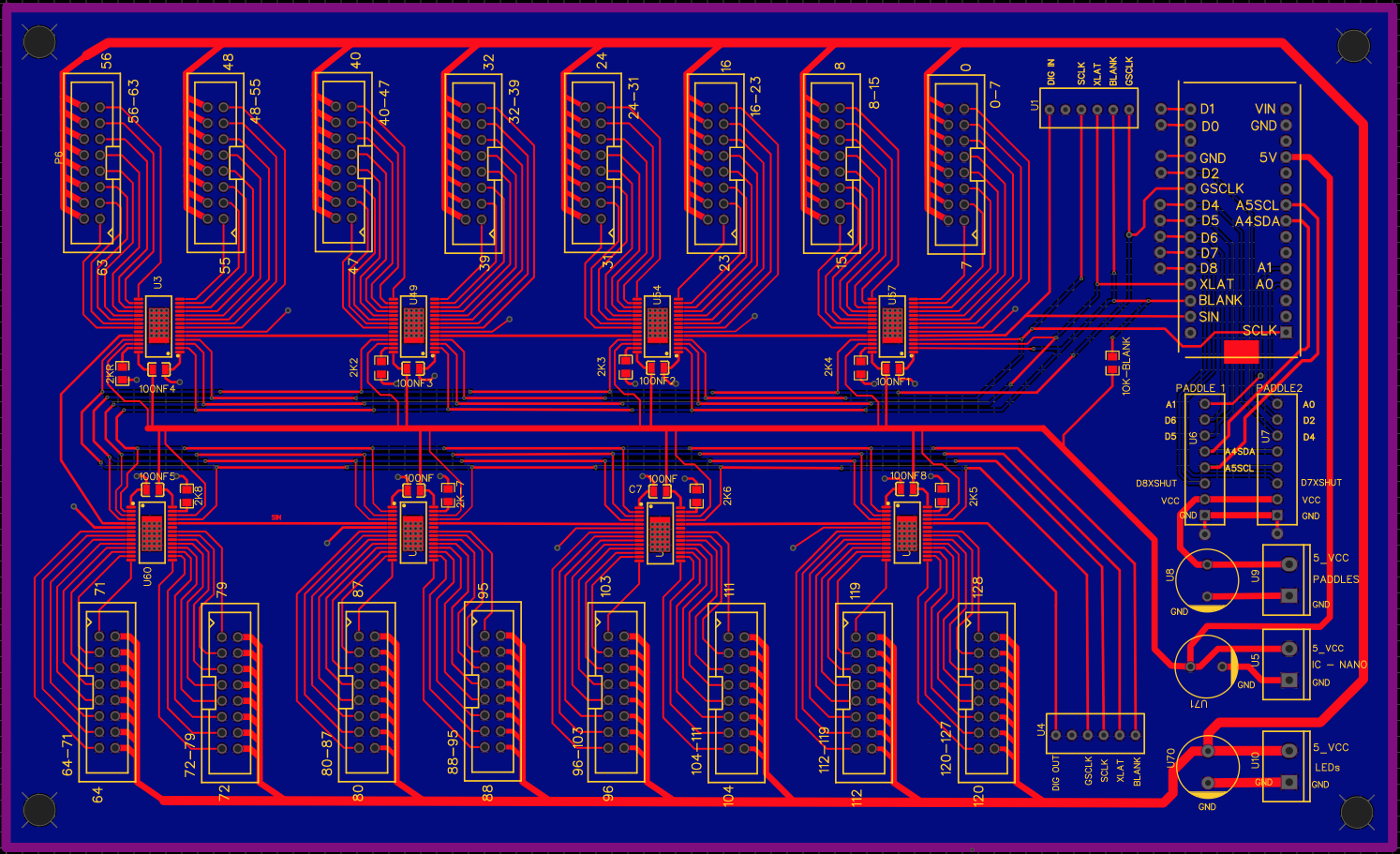
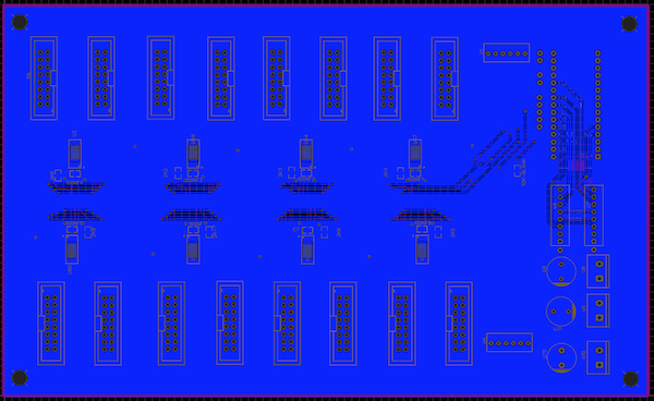
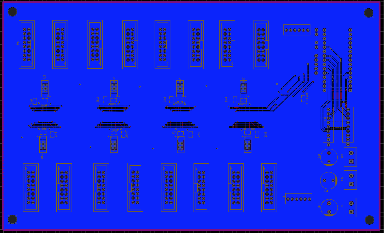
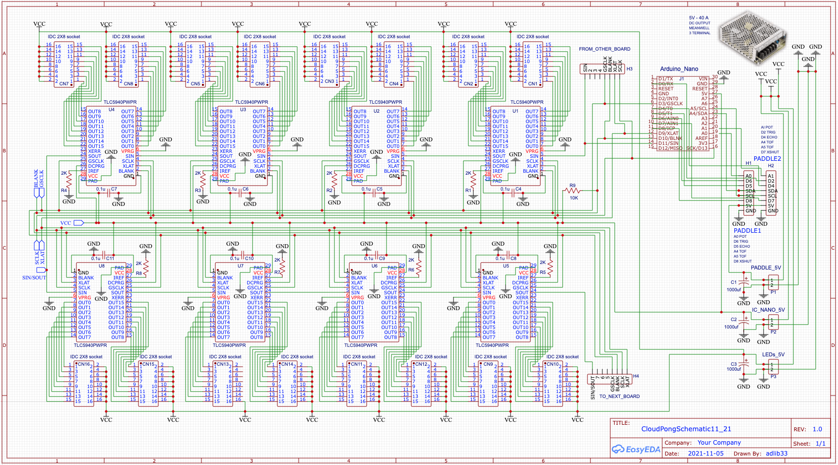
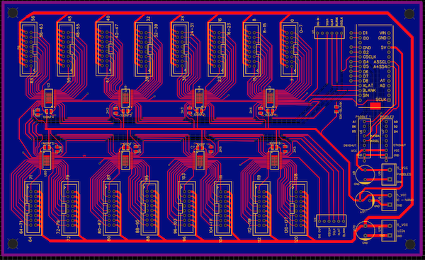
Effectively the board is a LED driver. It has a number of TLC5940 shift register ICs and their signal paths coming from an Arduino, the ICs control a large array of LEDs. There is a sensor input or two on the Arduino. Specifically, I’m trying to make sure that all of the grounds have a clean return path through the bottom copper layer. I’ve routed any and all GNDs (power, ICs, Arduino, Sensors) through vias to this bottom copper ground layer. As I understand it though, that is only half the battle.

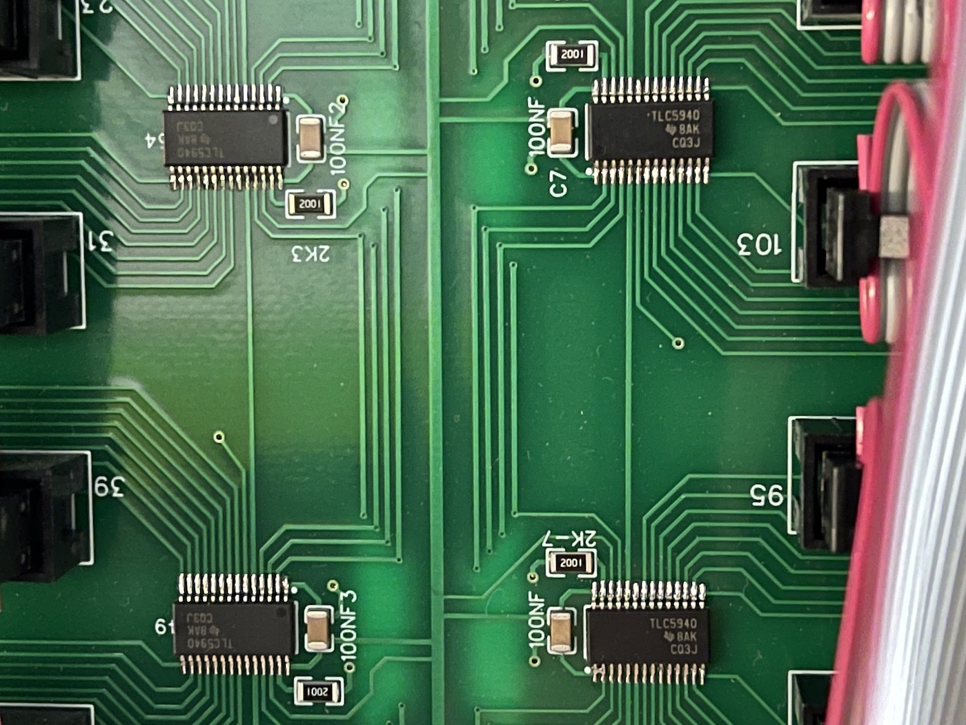
Power is getting to the Arduino and it is functioning. The sensors, though a long way away from board, are getting the required power and working. Ive tested the power bus traces out to the individual LEDs and they have enough voltage to do what they need to do when the power gets pulled down by the IC. I've had this circuit working with sixteen TLC5940/512 LEDs on a breadboard but now I'm getting nothing with these ICs on the PCB. Not even a flicker. The ICs just don't seem to be taking any power

My problems could be the board design itself, power management, or they could be my inability to solder those tiny little SMD components. Either way, I want to get the power/ground design checked/fixed before I send away for yet another set of boards, this time with Pick and Place.

BTW, I realize that this is a very inelegant solution for a LED driver, but it is the solution that I need nonetheless. It’s for an art installation that is already built, coded, so I have to make the circuits work as such.

Power - three 5V lines from a single 5V 40A Meanwell DC power supply. 5V line for the Sensors, 5V line for the Nano and ICs, and 5V line for the LEDs, separated and decoupled (I think)

IC’s - TLC5940 Shift Registers - TI Datasheet - https://www.ti.com/document-viewer/TLC5940/datasheet/pin_configuration_and_functions#SLVS5159151

Arduino Nano

Sensors - Using three different sensors to bring signals in and out of the Arduino via screw terminals. Per Sensors: The terminals and traces are close to the Nano.

PCB Design Back Ground Copper LayerBack_Copper_Layer Schematic for TLC5940 Board close-up SMD

[FIXED LINKS] The schematic for this circuit board on EasyEDA. Takes you to their sharing site OSHWLAB -

https://oshwlab.com/adlib33/cloudpongschematic11_21

The PCB - https://oshwlab.com/adlib33/cloudpongpcb

Looking for suggestions as to designing the ground layer of a PCB.

Effectively the board is a LED driver. It has a number of TLC5940 shift register ICs and their signal paths coming from an Arduino, the ICs control a large array of LEDs. There is a sensor input or two on the Arduino. Specifically, I’m trying to make sure that all of the grounds have a clean return path through the bottom copper layer. I’ve routed any and all GNDs (power, ICs, Arduino, Sensors) through vias to this bottom copper ground layer. As I understand it though, that is only half the battle.

Power is getting to the Arduino and it is functioning. The sensors, though a long way away from board, are getting the required power and working. Ive tested the power bus traces out to the individual LEDs and they have enough voltage to do what they need to do when the power gets pulled down by the IC. I've had this circuit working with sixteen TLC5940/512 LEDs on a breadboard but now I'm getting nothing with these ICs on the PCB. Not even a flicker. The ICs just don't seem to be taking any power

My problems could be the board design itself, power management, or they could be my inability to solder those tiny little SMD components. Either way, I want to get the power/ground design checked/fixed before I send away for yet another set of boards, this time with Pick and Place.

BTW, I realize that this is a very inelegant solution for a LED driver, but it is the solution that I need nonetheless. It’s for an art installation that is already built, coded, so I have to make the circuits work as such.

Power - three 5V lines from a single 5V 40A Meanwell DC power supply. 5V line for the Sensors, 5V line for the Nano and ICs, and 5V line for the LEDs, separated and decoupled (I think)

IC’s - TLC5940 Shift Registers - TI Datasheet - https://www.ti.com/document-viewer/TLC5940/datasheet/pin_configuration_and_functions#SLVS5159151

Arduino Nano

Sensors - Using three different sensors to bring signals in and out of the Arduino via screw terminals. Per Sensors: The terminals and traces are close to the Nano.

PCB Design Back Ground Copper Layer Schematic for TLC5940 Board close-up SMD

[FIXED LINKS] The schematic for this circuit board on EasyEDA. Takes you to their sharing site OSHWLAB -

https://oshwlab.com/adlib33/cloudpongschematic11_21

The PCB - https://oshwlab.com/adlib33/cloudpongpcb
Looking for suggestions as to designing the ground layer of a PCB.

Effectively the board is a LED driver. It has a number of TLC5940 shift register ICs and their signal paths coming from an Arduino, the ICs control a large array of LEDs. There is a sensor input or two on the Arduino. Specifically, I’m trying to make sure that all of the grounds have a clean return path through the bottom copper layer. I’ve routed any and all GNDs (power, ICs, Arduino, Sensors) through vias to this bottom copper ground layer. As I understand it though, that is only half the battle.

Power is getting to the Arduino and it is functioning. The sensors, though a long way away from board, are getting the required power and working. Ive tested the power bus traces out to the individual LEDs and they have enough voltage to do what they need to do when the power gets pulled down by the IC. I've had this circuit working with sixteen TLC5940/512 LEDs on a breadboard but now I'm getting nothing with these ICs on the PCB. Not even a flicker. The ICs just don't seem to be taking any power

My problems could be the board design itself, power management, or they could be my inability to solder those tiny little SMD components. Either way, I want to get the power/ground design checked/fixed before I send away for yet another set of boards, this time with Pick and Place.

BTW, I realize that this is a very inelegant solution for a LED driver, but it is the solution that I need nonetheless. It’s for an art installation that is already built, coded, so I have to make the circuits work as such.

Power - three 5V lines from a single 5V 40A Meanwell DC power supply. 5V line for the Sensors, 5V line for the Nano and ICs, and 5V line for the LEDs, separated and decoupled (I think)

IC’s - TLC5940 Shift Registers - TI Datasheet - https://www.ti.com/document-viewer/TLC5940/datasheet/pin_configuration_and_functions#SLVS5159151

Arduino Nano

Sensors - Using three different sensors to bring signals in and out of the Arduino via screw terminals. Per Sensors: The terminals and traces are close to the Nano.

PCB Design Back_Copper_Layer Schematic for TLC5940 Board close-up SMD

[FIXED LINKS] The schematic for this circuit board on EasyEDA. Takes you to their sharing site OSHWLAB -

https://oshwlab.com/adlib33/cloudpongschematic11_21

The PCB - https://oshwlab.com/adlib33/cloudpongpcb
added 89 characters in body
Source Link
adlib33e
  • 47
  • 2
  • 9

Looking for suggestions as to designing the ground layer of a PCB.

Effectively the board is a LED driver. It has a number of TLC5940 shift register ICs and their signal paths coming from an Arduino, the ICs control a large array of LEDs. There is a sensor input or two on the Arduino. Specifically, I’m trying to make sure that all of the grounds have a clean return path through the bottom copper layer. I’ve routed any and all GNDs (power, ICs, Arduino, Sensors) through vias to this bottom copper ground layer. As I understand it though, that is only half the battle.

Power is getting to the Arduino and it is functioning. The sensors, though a long way away from board, are getting the required power and working. Ive tested the power bus traces out to the individual LEDs and they have enough voltage to do what they need to do when the power gets pulled down by the IC. I've had this circuit working with sixteen TLC5940/512 LEDs on a breadboard but now I'm getting nothing with these ICs on the PCB. Not even a flicker. The ICs just don't seem to be taking any power

My problems could be the board design itself, power management, or they could be my inability to solder those tiny little SMD components. Either way, I want to get the power/ground design checked/fixed before I send away for yet another set of boards, this time with Pick and Place.

BTW, I realize that this is a very inelegant solution for a LED driver, but it is the solution that I need nonetheless. It’s for an art installation that is already built, coded, so I have to make the circuits work as such.

Power - three 5V lines from a single 5V 40A Meanwell DC power supply. 5V line for the Sensors, 5V line for the Nano and ICs, and 5V line for the LEDs, separated and decoupled (I think)

IC’s - TLC5940 Shift Registers - TI Datasheet - https://www.ti.com/document-viewer/TLC5940/datasheet/pin_configuration_and_functions#SLVS5159151

Arduino Nano

Sensors - Using three different sensors to bring signals in and out of the Arduino via screw terminals. Per Sensors: The terminals and traces are close to the Nano.

Front PCBPCB Design Back Ground Copper Layer SchematicSchematic for TLC5940 Board close-up SMD

[FIXED LINKS] The schematic for this circuit board on EasyEDA. Takes you to their sharing site OSHWLAB -

https://oshwlab.com/adlib33/cloudpongschematic11_21

The PCB - https://oshwlab.com/adlib33/cloudpongpcb
Looking for suggestions as to designing the ground layer of a PCB.

Effectively the board is a LED driver. It has a number of TLC5940 shift register ICs and their signal paths coming from an Arduino, the ICs control a large array of LEDs. There is a sensor input or two on the Arduino. Specifically, I’m trying to make sure that all of the grounds have a clean return path through the bottom copper layer. I’ve routed any and all GNDs (power, ICs, Arduino, Sensors) through vias to this bottom copper ground layer. As I understand it though, that is only half the battle.

Power is getting to the Arduino and it is functioning. The sensors, though a long way away from board, are getting the required power and working. Ive tested the power bus traces out to the individual LEDs and they have enough voltage to do what they need to do when the power gets pulled down by the IC. I've had this circuit working with sixteen TLC5940/512 LEDs on a breadboard but now I'm getting nothing with these ICs on the PCB. Not even a flicker. The ICs just don't seem to be taking any power

My problems could be the board design itself, power management, or they could be my inability to solder those tiny little SMD components. Either way, I want to get the power/ground design checked/fixed before I send away for yet another set of boards, this time with Pick and Place.

BTW, I realize that this is a very inelegant solution for a LED driver, but it is the solution that I need nonetheless. It’s for an art installation that is already built, coded, so I have to make the circuits work as such.

Power - three 5V lines from a single 5V 40A Meanwell DC power supply. 5V line for the Sensors, 5V line for the Nano and ICs, and 5V line for the LEDs, separated and decoupled (I think)

IC’s - TLC5940 Shift Registers - TI Datasheet - https://www.ti.com/document-viewer/TLC5940/datasheet/pin_configuration_and_functions#SLVS5159151

Arduino Nano

Sensors - Using three different sensors to bring signals in and out of the Arduino via screw terminals. Per Sensors: The terminals and traces are close to the Nano.

Front PCB Back Ground Copper Layer Schematic

[FIXED LINKS] The schematic for this circuit board on EasyEDA. Takes you to their sharing site OSHWLAB -

https://oshwlab.com/adlib33/cloudpongschematic11_21

The PCB - https://oshwlab.com/adlib33/cloudpongpcb
Looking for suggestions as to designing the ground layer of a PCB.

Effectively the board is a LED driver. It has a number of TLC5940 shift register ICs and their signal paths coming from an Arduino, the ICs control a large array of LEDs. There is a sensor input or two on the Arduino. Specifically, I’m trying to make sure that all of the grounds have a clean return path through the bottom copper layer. I’ve routed any and all GNDs (power, ICs, Arduino, Sensors) through vias to this bottom copper ground layer. As I understand it though, that is only half the battle.

Power is getting to the Arduino and it is functioning. The sensors, though a long way away from board, are getting the required power and working. Ive tested the power bus traces out to the individual LEDs and they have enough voltage to do what they need to do when the power gets pulled down by the IC. I've had this circuit working with sixteen TLC5940/512 LEDs on a breadboard but now I'm getting nothing with these ICs on the PCB. Not even a flicker. The ICs just don't seem to be taking any power

My problems could be the board design itself, power management, or they could be my inability to solder those tiny little SMD components. Either way, I want to get the power/ground design checked/fixed before I send away for yet another set of boards, this time with Pick and Place.

BTW, I realize that this is a very inelegant solution for a LED driver, but it is the solution that I need nonetheless. It’s for an art installation that is already built, coded, so I have to make the circuits work as such.

Power - three 5V lines from a single 5V 40A Meanwell DC power supply. 5V line for the Sensors, 5V line for the Nano and ICs, and 5V line for the LEDs, separated and decoupled (I think)

IC’s - TLC5940 Shift Registers - TI Datasheet - https://www.ti.com/document-viewer/TLC5940/datasheet/pin_configuration_and_functions#SLVS5159151

Arduino Nano

Sensors - Using three different sensors to bring signals in and out of the Arduino via screw terminals. Per Sensors: The terminals and traces are close to the Nano.

PCB Design Back Ground Copper Layer Schematic for TLC5940 Board close-up SMD

[FIXED LINKS] The schematic for this circuit board on EasyEDA. Takes you to their sharing site OSHWLAB -

https://oshwlab.com/adlib33/cloudpongschematic11_21

The PCB - https://oshwlab.com/adlib33/cloudpongpcb
added 37 characters in body
Source Link
adlib33e
  • 47
  • 2
  • 9

Looking for suggestions as to designing the ground layer of a PCB.

Effectively the board is a LED driver. It has a number of TLC5940 shift register ICs and their signal paths coming from an Arduino, the ICs control a large array of LEDs. There is a sensor input or two on the Arduino. Specifically, I’m trying to make sure that all of the grounds have a clean return path through the bottom copper layer. I’ve routed any and all GNDs (power, ICs, Arduino, Sensors) through vias to this bottom copper ground layer. As I understand it though, that is only half the battle.

Power is getting to the Arduino and it is functioning. The sensors, though a long way away from board, are getting the required power and working. Ive tested the power bus traces out to the individual LEDs and they have enough voltage to do what they need to do when the power gets pulled down by the IC. I've had this circuit working with sixteen TLC5940/512 LEDs on a breadboard but now I'm getting nothing with these ICs on the PCB. Not even a flicker. The ICs just don't seem to be taking any power

My problems could be the board design itself, power management, or they could be my inability to solder those tiny little SMD components. Either way, I want to get the power/ground design checked/fixed before I send away for yet another set of boards, this time with Pick and Place.

BTW, I realize that this is a very inelegant solution for a LED driver, but it is the solution that I need nonetheless. It’s for an art installation that is already built, coded, so I have to make the circuits work as such.

Power - three 5V lines from a single 5V 40A Meanwell DC power supply. 5V line for the Sensors, 5V line for the Nano and ICs, and 5V line for the LEDs, separated and decoupled (I think)

IC’s - TLC5940 Shift Registers - TI Datasheet - https://www.ti.com/document-viewer/TLC5940/datasheet/pin_configuration_and_functions#SLVS5159151

Arduino Nano

Sensors - Using three different sensors to bring signals in and out of the Arduino via screw terminals. Per Sensors: The terminals and traces are close to the Nano.

Front PCB Back Ground Copper Layer Schematic - works on a breadboardSchematic

[FIXED LINKS] The schematic for this circuit board on EasyEDA. Takes you to their sharing site OSHWLAB - https://easyeda.com/adlib33/cloudpongschematic11_21 The

https://oshwlab.com/adlib33/cloudpongschematic11_21

The PCB - https://easyeda.com/adlib33/cloudpongpcbhttps://oshwlab.com/adlib33/cloudpongpcb

Looking for suggestions as to designing the ground layer of a PCB.

Effectively the board is a LED driver. It has a number of TLC5940 shift register ICs and their signal paths coming from an Arduino, the ICs control a large array of LEDs. There is a sensor input or two on the Arduino. Specifically, I’m trying to make sure that all of the grounds have a clean return path through the bottom copper layer. I’ve routed any and all GNDs (power, ICs, Arduino, Sensors) through vias to this bottom copper ground layer. As I understand it though, that is only half the battle.

Power is getting to the Arduino and it is functioning. The sensors, though a long way away from board, are getting the required power and working. Ive tested the power bus traces out to the individual LEDs and they have enough voltage to do what they need to do when the power gets pulled down by the IC. I've had this circuit working with sixteen TLC5940/512 LEDs on a breadboard but now I'm getting nothing with these ICs on the PCB. Not even a flicker. The ICs just don't seem to be taking any power

My problems could be the board design itself, power management, or they could be my inability to solder those tiny little SMD components. Either way, I want to get the power/ground design checked/fixed before I send away for yet another set of boards, this time with Pick and Place.

BTW, I realize that this is a very inelegant solution for a LED driver, but it is the solution that I need nonetheless. It’s for an art installation that is already built, coded, so I have to make the circuits work as such.

Power - three 5V lines from a single 5V 40A Meanwell DC power supply. 5V line for the Sensors, 5V line for the Nano and ICs, and 5V line for the LEDs, separated and decoupled (I think)

IC’s - TLC5940 Shift Registers - TI Datasheet - https://www.ti.com/document-viewer/TLC5940/datasheet/pin_configuration_and_functions#SLVS5159151

Arduino Nano

Sensors - Using three different sensors to bring signals in and out of the Arduino via screw terminals. Per Sensors: The terminals and traces are close to the Nano.

Front PCB Back Ground Copper Layer Schematic - works on a breadboard

The schematic for this circuit board on EasyEDA - https://easyeda.com/adlib33/cloudpongschematic11_21 The PCB - https://easyeda.com/adlib33/cloudpongpcb

Looking for suggestions as to designing the ground layer of a PCB.

Effectively the board is a LED driver. It has a number of TLC5940 shift register ICs and their signal paths coming from an Arduino, the ICs control a large array of LEDs. There is a sensor input or two on the Arduino. Specifically, I’m trying to make sure that all of the grounds have a clean return path through the bottom copper layer. I’ve routed any and all GNDs (power, ICs, Arduino, Sensors) through vias to this bottom copper ground layer. As I understand it though, that is only half the battle.

Power is getting to the Arduino and it is functioning. The sensors, though a long way away from board, are getting the required power and working. Ive tested the power bus traces out to the individual LEDs and they have enough voltage to do what they need to do when the power gets pulled down by the IC. I've had this circuit working with sixteen TLC5940/512 LEDs on a breadboard but now I'm getting nothing with these ICs on the PCB. Not even a flicker. The ICs just don't seem to be taking any power

My problems could be the board design itself, power management, or they could be my inability to solder those tiny little SMD components. Either way, I want to get the power/ground design checked/fixed before I send away for yet another set of boards, this time with Pick and Place.

BTW, I realize that this is a very inelegant solution for a LED driver, but it is the solution that I need nonetheless. It’s for an art installation that is already built, coded, so I have to make the circuits work as such.

Power - three 5V lines from a single 5V 40A Meanwell DC power supply. 5V line for the Sensors, 5V line for the Nano and ICs, and 5V line for the LEDs, separated and decoupled (I think)

IC’s - TLC5940 Shift Registers - TI Datasheet - https://www.ti.com/document-viewer/TLC5940/datasheet/pin_configuration_and_functions#SLVS5159151

Arduino Nano

Sensors - Using three different sensors to bring signals in and out of the Arduino via screw terminals. Per Sensors: The terminals and traces are close to the Nano.

Front PCB Back Ground Copper Layer Schematic

[FIXED LINKS] The schematic for this circuit board on EasyEDA. Takes you to their sharing site OSHWLAB -

https://oshwlab.com/adlib33/cloudpongschematic11_21

The PCB - https://oshwlab.com/adlib33/cloudpongpcb
added 444 characters in body
Source Link
adlib33e
  • 47
  • 2
  • 9
Loading
Source Link
adlib33e
  • 47
  • 2
  • 9
Loading