Became Hot Network Question
Tweeted twitter.com/StackElectronix/status/1517971590939561991
tweaked why I was unsure of the power supply filtering idea.
Source Link

I have an FPGA dev board with a fan PWM circuit so that you can hook it up to a fan + heatsink. I happen to like this as we put a common heatsink together for the hottest components, and I drive it from the FPGA based on the FPGA's internal temp.

Now we're looking to build the first iteration of our own PCB. I have made a "highlights" schematic showing basic connectivity and some of the support circuits for elements outside the FPGA. I will soon be handing this schematic to our real electrical engineer. The fan PWM support circuit is one on my "quasischematic," and I basically had to reproduce it from the dev board's schematic. Shown here:

FanPWM Circuit

I think I understand most of this. R8, R9, R10, and Q1 are there to take the relatively small CMOS 3.3V signal of the FPGA (FanPWM) and turn it into something high enough current to drive the power MOSFET. R7 is a current limiting resistor, preventing a 100% duty cycle from letting the fan draw more current than it can handle. Q2 is the power MOSFET that acts like the "on-off" switch that sits between the fan and the ground.

Here's the part I am confused about. What is the reason for the Schottky rectifier and the polarized capacitor? I only have one idea about the diode, which seems odd to me. The capacitor I have two ideas, but neither seems right.

Diode Idea: ESD So I thought that maybe the diode was for some static protection between 12V and the other stuff. But that seems odd because, without it, the fan should act as a large inductor any instantaneous spike due to ESD or inrush current when the 12V supply is connected should be stopped by the fan, and frankly, anything not blocked by the fan will bypass the diode anyways.

Capacitor Idea 1: Power Supply Filtering This idea seems unlikely because the capacitor is polarized, has a relatively large value, and is not in parallel with at least one other cap. The other power supply filtering capacitor arrangements I see elsewhere are frequently 10uF in parallel with 0.1uF or 2.2uF with 10nF. Here we might have low frequency covered but not high frequency, and the polarization is odd. Further, this is not between 12V and ground.

Capacitor Idea 2: Energy Storage / Pulse Smoothing I thought maybe a large capacitor like that might be storing energy to "smooth out" the sharp pulse edges. But that seems odd to me as this is on the ground side of the fan.

So my question is: what is the purpose of the diode and capacitor in this circuit?

I have an FPGA dev board with a fan PWM circuit so that you can hook it up to a fan + heatsink. I happen to like this as we put a common heatsink together for the hottest components, and I drive it from the FPGA based on the FPGA's internal temp.

Now we're looking to build the first iteration of our own PCB. I have made a "highlights" schematic showing basic connectivity and some of the support circuits for elements outside the FPGA. I will soon be handing this schematic to our real electrical engineer. The fan PWM support circuit is one on my "quasischematic," and I basically had to reproduce it from the dev board's schematic. Shown here:

FanPWM Circuit

I think I understand most of this. R8, R9, R10, and Q1 are there to take the relatively small CMOS 3.3V signal of the FPGA (FanPWM) and turn it into something high enough current to drive the power MOSFET. R7 is a current limiting resistor, preventing a 100% duty cycle from letting the fan draw more current than it can handle. Q2 is the power MOSFET that acts like the "on-off" switch that sits between the fan and the ground.

Here's the part I am confused about. What is the reason for the Schottky rectifier and the polarized capacitor? I only have one idea about the diode, which seems odd to me. The capacitor I have two ideas, but neither seems right.

Diode Idea: ESD So I thought that maybe the diode was for some static protection between 12V and the other stuff. But that seems odd because, without it, the fan should act as a large inductor any instantaneous spike due to ESD or inrush current when the 12V supply is connected should be stopped by the fan, and frankly, anything not blocked by the fan will bypass the diode anyways.

Capacitor Idea 1: Power Supply Filtering This idea seems unlikely because the capacitor is polarized, has a relatively large value, and is not in parallel with at least one other cap. The other power supply filtering capacitor arrangements I see elsewhere are frequently 10uF in parallel with 0.1uF or 2.2uF with 10nF. Here we might have low frequency covered but not high frequency, and the polarization is odd.

Capacitor Idea 2: Energy Storage / Pulse Smoothing I thought maybe a large capacitor like that might be storing energy to "smooth out" the sharp pulse edges. But that seems odd to me as this is on the ground side of the fan.

So my question is: what is the purpose of the diode and capacitor in this circuit?
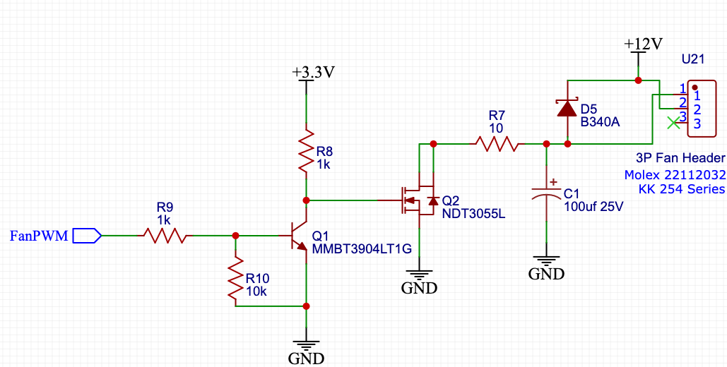
I have an FPGA dev board with a fan PWM circuit so that you can hook it up to a fan + heatsink. I happen to like this as we put a common heatsink together for the hottest components, and I drive it from the FPGA based on the FPGA's internal temp.

Now we're looking to build the first iteration of our own PCB. I have made a "highlights" schematic showing basic connectivity and some of the support circuits for elements outside the FPGA. I will soon be handing this schematic to our real electrical engineer. The fan PWM support circuit is one on my "quasischematic," and I basically had to reproduce it from the dev board's schematic. Shown here:

FanPWM Circuit

I think I understand most of this. R8, R9, R10, and Q1 are there to take the relatively small CMOS 3.3V signal of the FPGA (FanPWM) and turn it into something high enough current to drive the power MOSFET. R7 is a current limiting resistor, preventing a 100% duty cycle from letting the fan draw more current than it can handle. Q2 is the power MOSFET that acts like the "on-off" switch that sits between the fan and the ground.

Here's the part I am confused about. What is the reason for the Schottky rectifier and the polarized capacitor? I only have one idea about the diode, which seems odd to me. The capacitor I have two ideas, but neither seems right.

Diode Idea: ESD So I thought that maybe the diode was for some static protection between 12V and the other stuff. But that seems odd because, without it, the fan should act as a large inductor any instantaneous spike due to ESD or inrush current when the 12V supply is connected should be stopped by the fan, and frankly, anything not blocked by the fan will bypass the diode anyways.

Capacitor Idea 1: Power Supply Filtering This idea seems unlikely because the capacitor is polarized, has a relatively large value, and is not in parallel with at least one other cap. The other power supply filtering capacitor arrangements I see elsewhere are frequently 10uF in parallel with 0.1uF or 2.2uF with 10nF. Here we might have low frequency covered but not high frequency, and the polarization is odd. Further, this is not between 12V and ground.

Capacitor Idea 2: Energy Storage / Pulse Smoothing I thought maybe a large capacitor like that might be storing energy to "smooth out" the sharp pulse edges. But that seems odd to me as this is on the ground side of the fan.

So my question is: what is the purpose of the diode and capacitor in this circuit?

Source Link

What is the purpose of the capacitor and diode in this fan driver circuit?

I have an FPGA dev board with a fan PWM circuit so that you can hook it up to a fan + heatsink. I happen to like this as we put a common heatsink together for the hottest components, and I drive it from the FPGA based on the FPGA's internal temp.

Now we're looking to build the first iteration of our own PCB. I have made a "highlights" schematic showing basic connectivity and some of the support circuits for elements outside the FPGA. I will soon be handing this schematic to our real electrical engineer. The fan PWM support circuit is one on my "quasischematic," and I basically had to reproduce it from the dev board's schematic. Shown here:

FanPWM Circuit

I think I understand most of this. R8, R9, R10, and Q1 are there to take the relatively small CMOS 3.3V signal of the FPGA (FanPWM) and turn it into something high enough current to drive the power MOSFET. R7 is a current limiting resistor, preventing a 100% duty cycle from letting the fan draw more current than it can handle. Q2 is the power MOSFET that acts like the "on-off" switch that sits between the fan and the ground.

Here's the part I am confused about. What is the reason for the Schottky rectifier and the polarized capacitor? I only have one idea about the diode, which seems odd to me. The capacitor I have two ideas, but neither seems right.

Diode Idea: ESD So I thought that maybe the diode was for some static protection between 12V and the other stuff. But that seems odd because, without it, the fan should act as a large inductor any instantaneous spike due to ESD or inrush current when the 12V supply is connected should be stopped by the fan, and frankly, anything not blocked by the fan will bypass the diode anyways.

Capacitor Idea 1: Power Supply Filtering This idea seems unlikely because the capacitor is polarized, has a relatively large value, and is not in parallel with at least one other cap. The other power supply filtering capacitor arrangements I see elsewhere are frequently 10uF in parallel with 0.1uF or 2.2uF with 10nF. Here we might have low frequency covered but not high frequency, and the polarization is odd.

Capacitor Idea 2: Energy Storage / Pulse Smoothing I thought maybe a large capacitor like that might be storing energy to "smooth out" the sharp pulse edges. But that seems odd to me as this is on the ground side of the fan.

So my question is: what is the purpose of the diode and capacitor in this circuit?