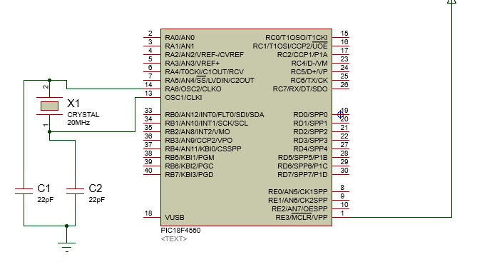
I am trying to add a 20MHz external crystal oscillator to my PIC18F4550 microcontroller. The external crystal oscillator circuit connections to the PIC18F4450 is as below:

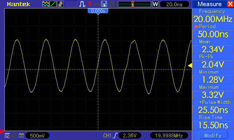
The Datasheet suggest to use 15pF capacitors for 20MHz crystal however, I have used 22pF by mistake. With that said, when I try to hook up my oscilloscope to check the PIN13 (OSC1) of PIC18 microcontroller, I am able to see the 20MHz sine wave signal present as below. So I decided against replacing the existing 22pF capacitors with 15pF capacitors.

Then, I used the following code to create a shortest pulse width possible at LATB7.
// PIC18F4550 Configuration Bit Settings

// 'C' source line config statements

// CONFIG1L
#pragma config PLLDIV = 5       // PLL Prescaler Selection bits (No prescale (4 MHz oscillator input drives PLL directly))
#pragma config CPUDIV = OSC1_PLL2// System Clock Postscaler Selection bits ([Primary Oscillator Src: /1][96 MHz PLL Src: /2])
#pragma config USBDIV = 1       // USB Clock Selection bit (used in Full-Speed USB mode only; UCFG:FSEN = 1) (USB clock source comes directly from the primary oscillator block with no postscale)

// CONFIG1H
#pragma config FOSC = HS // Oscillator Selection bits (Internal oscillator, HS oscillator used by USB (INTHS))
#pragma config FCMEN = OFF      // Fail-Safe Clock Monitor Enable bit (Fail-Safe Clock Monitor disabled)
#pragma config IESO = OFF       // Internal/External Oscillator Switchover bit (Oscillator Switchover mode disabled)

// CONFIG2L
#pragma config PWRT = OFF       // Power-up Timer Enable bit (PWRT disabled)
#pragma config BOR = ON         // Brown-out Reset Enable bits (Brown-out Reset enabled in hardware only (SBOREN is disabled))
#pragma config BORV = 3         // Brown-out Reset Voltage bits (Minimum setting 2.05V)
#pragma config VREGEN = OFF     // USB Voltage Regulator Enable bit (USB voltage regulator disabled)

// CONFIG2H
#pragma config WDT = OFF         // Watchdog Timer Enable bit (WDT enabled)
#pragma config WDTPS = 32768    // Watchdog Timer Postscale Select bits (1:32768)

// CONFIG3H
#pragma config CCP2MX = ON      // CCP2 MUX bit (CCP2 input/output is multiplexed with RC1)
#pragma config PBADEN = ON      // PORTB A/D Enable bit (PORTB<4:0> pins are configured as analog input channels on Reset)
#pragma config LPT1OSC = OFF    // Low-Power Timer 1 Oscillator Enable bit (Timer1 configured for higher power operation)
#pragma config MCLRE = ON       // MCLR Pin Enable bit (MCLR pin enabled; RE3 input pin disabled)

// CONFIG4L
#pragma config STVREN = ON      // Stack Full/Underflow Reset Enable bit (Stack full/underflow will cause Reset)
#pragma config LVP = OFF         // Single-Supply ICSP Enable bit (Single-Supply ICSP enabled)
#pragma config ICPRT = OFF      // Dedicated In-Circuit Debug/Programming Port (ICPORT) Enable bit (ICPORT disabled)
#pragma config XINST = OFF      // Extended Instruction Set Enable bit (Instruction set extension and Indexed Addressing mode disabled (Legacy mode))

// CONFIG5L
#pragma config CP0 = OFF        // Code Protection bit (Block 0 (000800-001FFFh) is not code-protected)
#pragma config CP1 = OFF        // Code Protection bit (Block 1 (002000-003FFFh) is not code-protected)
#pragma config CP2 = OFF        // Code Protection bit (Block 2 (004000-005FFFh) is not code-protected)
#pragma config CP3 = OFF        // Code Protection bit (Block 3 (006000-007FFFh) is not code-protected)

// CONFIG5H
#pragma config CPB = OFF        // Boot Block Code Protection bit (Boot block (000000-0007FFh) is not code-protected)
#pragma config CPD = OFF        // Data EEPROM Code Protection bit (Data EEPROM is not code-protected)

// CONFIG6L
#pragma config WRT0 = OFF       // Write Protection bit (Block 0 (000800-001FFFh) is not write-protected)
#pragma config WRT1 = OFF       // Write Protection bit (Block 1 (002000-003FFFh) is not write-protected)
#pragma config WRT2 = OFF       // Write Protection bit (Block 2 (004000-005FFFh) is not write-protected)
#pragma config WRT3 = OFF       // Write Protection bit (Block 3 (006000-007FFFh) is not write-protected)

// CONFIG6H
#pragma config WRTC = OFF       // Configuration Register Write Protection bit (Configuration registers (300000-3000FFh) are not write-protected)
#pragma config WRTB = OFF       // Boot Block Write Protection bit (Boot block (000000-0007FFh) is not write-protected)
#pragma config WRTD = OFF       // Data EEPROM Write Protection bit (Data EEPROM is not write-protected)

// CONFIG7L
#pragma config EBTR0 = OFF      // Table Read Protection bit (Block 0 (000800-001FFFh) is not protected from table reads executed in other blocks)
#pragma config EBTR1 = OFF      // Table Read Protection bit (Block 1 (002000-003FFFh) is not protected from table reads executed in other blocks)
#pragma config EBTR2 = OFF      // Table Read Protection bit (Block 2 (004000-005FFFh) is not protected from table reads executed in other blocks)
#pragma config EBTR3 = OFF      // Table Read Protection bit (Block 3 (006000-007FFFh) is not protected from table reads executed in other blocks)

// CONFIG7H
#pragma config EBTRB = OFF      // Boot Block Table Read Protection bit (Boot block (000000-0007FFh) is not protected from table reads executed in other blocks)

// #pragma config statements should precede project file includes.
// Use project enums instead of #define for ON and OFF.

#include <xc.h>
#include <pic18f4550.h>

#define _XTAL_FREQ 20000000
#define LED LATBbits.LATB7
#define ON 1
#define OFF 0

void main(void) {
    TRISBbits.TRISB7 = 0;
    while(1)
     {
        LED = ON;
        NOP();
        LED = OFF;
     }
     }
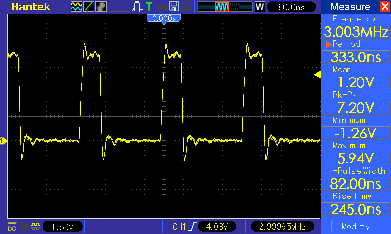
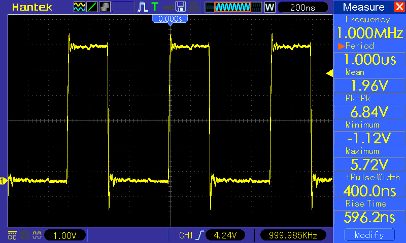
However, when I monitor the output pin RB7 with oscilloscope, it appears the the pulse width is around 400ns.

Since the frequency is 20MHz, each cycle would be 50ns. Assuming PIC18F4550 need 4 clock cycles for 1 instruction cycle, shouldn't I be able to achieve a lower pulse width than 400ns? What am I missing?

