deleted 14 characters in body
Source Link
Voltage Spike
  • 88.8k
  • 49
  • 90
  • 234

enter image description here

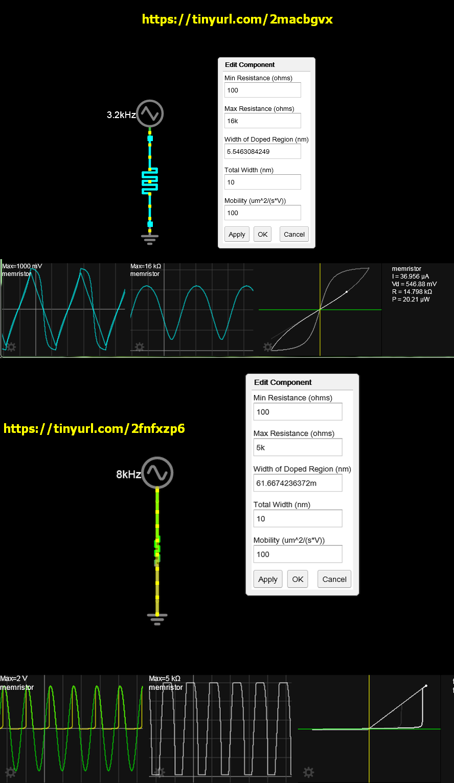
That physically means you do not have a memristor which have passive magnetic properties that are symmetrical in polarity. That is until a threshold voltage then they conduct heavily and behave like linear resistance until the polarity is sufficient reversed. This creates a pulsed current with a linear R on voltage modulation until 0V then high impedance again on negative polarities.

The dynamic range of resistance depends on the physical properties of the doped region in length and width in nm. the area of the curve maximizes memory from hysteresis whereas a resistor has no VI loop area.

So excessive voltage will cause the spike property. Seen below with excess voltage. enter image description here
Yet a capacitor and a diode have this similar property or a diode partially blown by ESD with lower R and higher C from the small gap. LEDs have this property when wounded by ESD but still work.

Adding DC bias does not simulate your hypothetical question as the amount of heavy conduction and nonlinear spike current requires a certain percentage of negative bias to regain the positive VI memory loop.

V = X axis , I = Y axis vertical.

enter image description here

  1. Theta increases with conduction [S] since the slope represents mean resistance V/I=R . Higher conduction occurs with higher voltage and current until the breakdown voltage trigger level is reached then causes spike current. This is physically determined by geometry of the gap size and doping thickness.

You can see this on my simulation but the plot needs to be manually resized if spike response occurs.

3.

What about area or ellipical shape as you showed.

enter image description here

The area is proportional to the magnetic constant of partial permeability or the hysteresis of margin from detecting current during rising and falling voltage.

But stretching the ellipse does not change the area so that does not show any memory gain margin.

Other opinions

OTP programmable static memories have a dynamic ratio of impedance of over 5 decades that depend on almost zero leakage current integrated over 10 years. While Memristors have a practical dynamic range of 2 to 3 decades and an inherent junction capacitance that limits frequency response to several decades below semiconductor OTP memory or EPROM due to the 2 or 3 orders of higher resistance.

Any Questions?

enter image description here

That physically means you do not have a memristor which have passive magnetic properties that are symmetrical in polarity. That is until a threshold voltage then they conduct heavily and behave like linear resistance until the polarity is sufficient reversed. This creates a pulsed current with a linear R on voltage modulation until 0V then high impedance again on negative polarities.

The dynamic range of resistance depends on the physical properties of the doped region in length and width in nm. the area of the curve maximizes memory from hysteresis whereas a resistor has no VI loop area.

So excessive voltage will cause the spike property. Seen below with excess voltage. enter image description here

Yet a capacitor and a diode have this similar property or a diode partially blown by ESD with lower R and higher C from the small gap. LEDs have this property when wounded by ESD but still work.

Adding DC bias does not simulate your hypothetical question as the amount of heavy conduction and nonlinear spike current requires a certain percentage of negative bias to regain the positive VI memory loop.

V = X axis , I = Y axis vertical.

enter image description here

  1. Theta increases with conduction [S] since the slope represents mean resistance V/I=R . Higher conduction occurs with higher voltage and current until the breakdown voltage trigger level is reached then causes spike current. This is physically determined by geometry of the gap size and doping thickness.

You can see this on my simulation but the plot needs to be manually resized if spike response occurs.

3.

What about area or ellipical shape as you showed.

enter image description here

The area is proportional to the magnetic constant of partial permeability or the hysteresis of margin from detecting current during rising and falling voltage.

But stretching the ellipse does not change the area so that does not show any memory gain margin.

Other opinions

OTP programmable static memories have a dynamic ratio of impedance of over 5 decades that depend on almost zero leakage current integrated over 10 years. While Memristors have a practical dynamic range of 2 to 3 decades and an inherent junction capacitance that limits frequency response to several decades below semiconductor OTP memory or EPROM due to the 2 or 3 orders of higher resistance.

Any Questions?
enter image description here

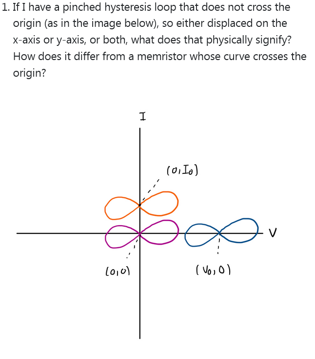
That physically means you do not have a memristor which have passive magnetic properties that are symmetrical in polarity. That is until a threshold voltage then they conduct heavily and behave like linear resistance until the polarity is sufficient reversed. This creates a pulsed current with a linear R on voltage modulation until 0V then high impedance again on negative polarities.

The dynamic range of resistance depends on the physical properties of the doped region in length and width in nm. the area of the curve maximizes memory from hysteresis whereas a resistor has no VI loop area.

So excessive voltage will cause the spike property. Seen below with excess voltage. enter image description here

Yet a capacitor and a diode have this similar property or a diode partially blown by ESD with lower R and higher C from the small gap. LEDs have this property when wounded by ESD but still work.

Adding DC bias does not simulate your hypothetical question as the amount of heavy conduction and nonlinear spike current requires a certain percentage of negative bias to regain the positive VI memory loop.

V = X axis , I = Y axis vertical.

enter image description here

  1. Theta increases with conduction [S] since the slope represents mean resistance V/I=R . Higher conduction occurs with higher voltage and current until the breakdown voltage trigger level is reached then causes spike current. This is physically determined by geometry of the gap size and doping thickness.

You can see this on my simulation but the plot needs to be manually resized if spike response occurs.

3.

What about area or ellipical shape as you showed.

enter image description here

The area is proportional to the magnetic constant of partial permeability or the hysteresis of margin from detecting current during rising and falling voltage.

But stretching the ellipse does not change the area so that does not show any memory gain margin.

Other opinions

OTP programmable static memories have a dynamic ratio of impedance of over 5 decades that depend on almost zero leakage current integrated over 10 years. While Memristors have a practical dynamic range of 2 to 3 decades and an inherent junction capacitance that limits frequency response to several decades below semiconductor OTP memory or EPROM due to the 2 or 3 orders of higher resistance.

added 175 characters in body
Source Link
D.A.S.
  • 148k
  • 3
  • 56
  • 190

enter image description here

That physically means you do not have a memristor which have passive magnetic properties that are symmetrical in polarity. That is until a threshold voltage then they conduct heavily and behave like linear resistance until the polarity is sufficient reversed. This creates a pulsed current with a linear R on voltage modulation until 0V then high impedance again on negative polarities.

The dynamic range of resistance depends on the physical properties of the doped region in length and width in nm. the area of the curve maximizes memory from hysteresis whereas a resistor has no VI loop area.

So excessive voltage will cause the spike property. Seen below with excess voltage. enter image description here

Yet a capacitor and a diode have this similar property or a diode partially blown by ESD with lower R and higher C from the small gap. LEDs have this property when wounded by ESD but still work.

Adding DC bias does not simulate your hypothetical question as the amount of heavy conduction and nonlinear spike current requires a certain percentage of negative bias to regain the positive VI memory loop.

V = X axis , I = Y axis vertical.

enter image description here

  1. Theta increases with conduction or[S] since the slope represents mean resistance V/I=R . Higher conduction occurs with higher voltage and current until the breakdown voltage trigger level foris reached then causes spike current due to. This is physically determined by geometry of the gap size and doping thickness.

You can see this on my simulation but the plot needs to be manually resized if spike response occurs.

3.

What about area or ellipical shape as you showed.

enter image description here

The area is proportional to the magnetic constant of partial permeability or the hysteresis of margin from detecting current during rising and falling voltage.

But stretching the ellipse does not change the area so that does not show any memory gain margin.

Other opinions

OTP programmable static memories have a dynamic ratio of impedance of over 5 decades that depend on almost zero leakage current integrated over 10 years. While Memristors have a practical dynamic range of 2 to 3 decades and an inherent junction capacitance that limits frequency response to several decades below semiconductor OTP memory or EPROM due to the 2 or 3 orders of higher resistance.

Any Questions?
enter image description here

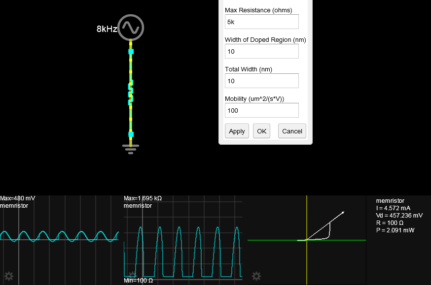
That physically means you do not have a memristor which have passive magnetic properties that are symmetrical in polarity. That is until a threshold voltage then they conduct heavily and behave like linear resistance until the polarity is sufficient reversed. This creates a pulsed current with a linear R on voltage modulation until 0V then high impedance again on negative polarities.

The dynamic range of resistance depends on the physical properties of the doped region in length and width in nm. the area of the curve maximizes memory from hysteresis whereas a resistor has no VI loop area.

So excessive voltage will cause the spike property. Seen below with excess voltage. enter image description here

Yet a capacitor and a diode have this similar property or a diode partially blown by ESD with lower R and higher C from the small gap. LEDs have this property when wounded by ESD but still work.

Adding DC bias does not simulate your hypothetical question as the amount of heavy conduction and nonlinear spike current requires a certain percentage of negative bias to regain the positive VI memory loop.

V = X axis , I = Y axis vertical.

enter image description here

  1. Theta increases with conduction or higher voltage and current until the breakdown voltage trigger level for spike current due to gap size and doping.

You can see this on my simulation but the plot needs to be manually resized if spike response occurs.

3.

What about area or ellipical shape as you showed.

enter image description here

The area is proportional to the magnetic constant of partial permeability or the hysteresis of margin from detecting current during rising and falling voltage.

But stretching the ellipse does not change the area so that does not show any memory gain margin.

Other opinions

OTP programmable static memories have a dynamic ratio of impedance of over 5 decades that depend on almost zero leakage current integrated over 10 years. While Memristors have a practical dynamic range of 2 to 3 decades and an inherent junction capacitance that limits frequency response to several decades below semiconductor OTP memory or EPROM due to the 2 or 3 orders of higher resistance.

enter image description here

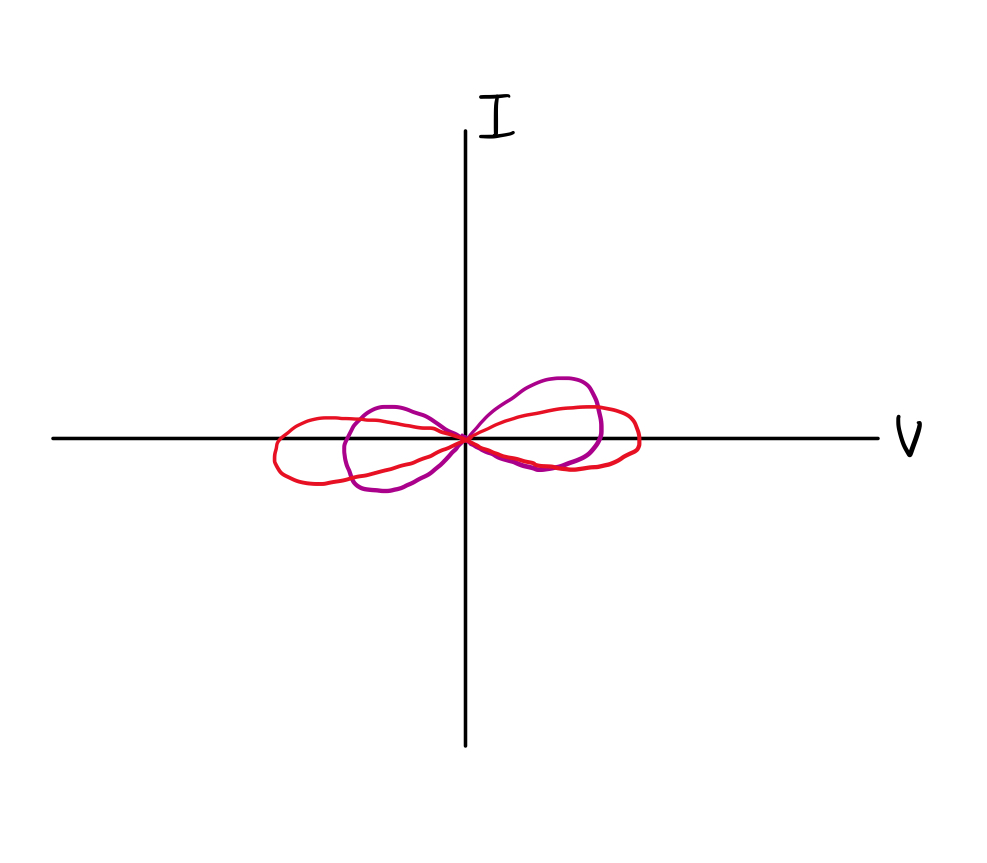
That physically means you do not have a memristor which have passive magnetic properties that are symmetrical in polarity. That is until a threshold voltage then they conduct heavily and behave like linear resistance until the polarity is sufficient reversed. This creates a pulsed current with a linear R on voltage modulation until 0V then high impedance again on negative polarities.

The dynamic range of resistance depends on the physical properties of the doped region in length and width in nm. the area of the curve maximizes memory from hysteresis whereas a resistor has no VI loop area.

So excessive voltage will cause the spike property. Seen below with excess voltage. enter image description here

Yet a capacitor and a diode have this similar property or a diode partially blown by ESD with lower R and higher C from the small gap. LEDs have this property when wounded by ESD but still work.

Adding DC bias does not simulate your hypothetical question as the amount of heavy conduction and nonlinear spike current requires a certain percentage of negative bias to regain the positive VI memory loop.

V = X axis , I = Y axis vertical.

enter image description here

  1. Theta increases with conduction [S] since the slope represents mean resistance V/I=R . Higher conduction occurs with higher voltage and current until the breakdown voltage trigger level is reached then causes spike current. This is physically determined by geometry of the gap size and doping thickness.

You can see this on my simulation but the plot needs to be manually resized if spike response occurs.

3.

What about area or ellipical shape as you showed.

enter image description here

The area is proportional to the magnetic constant of partial permeability or the hysteresis of margin from detecting current during rising and falling voltage.

But stretching the ellipse does not change the area so that does not show any memory gain margin.

Other opinions

OTP programmable static memories have a dynamic ratio of impedance of over 5 decades that depend on almost zero leakage current integrated over 10 years. While Memristors have a practical dynamic range of 2 to 3 decades and an inherent junction capacitance that limits frequency response to several decades below semiconductor OTP memory or EPROM due to the 2 or 3 orders of higher resistance.

Any Questions?
added 1093 characters in body
Source Link
D.A.S.
  • 148k
  • 3
  • 56
  • 190

enter image description here

That physically means you do not have a memristor which have passive magnetic properties that are symmetrical in polarity. That is until a threshold voltage then they conduct heavily and behave like linear resistance until the polarity is sufficient reversed. This creates a pulsed current with a linear R on voltage modulation until 0V then high impedance again on negative polarities.

The dynamic range of resistance depends on the physical properties of the doped region in length and width in nm. the area of the curve maximizes memory from hysteresis whereas a resistor has no VI loop area.

So excessive voltage will cause the spike property. Seen below with excess voltage. enter image description here

Yet a capacitor and a diode have this similar property or a diode partially blown by ESD with lower R and higher C from the small gap. LEDs have this property when wounded by ESD but still work.

Adding DC bias does not simulate your hypothetical question as the amount of heavy conduction and nonlinear spike current requires a certain percentage of negative bias to regain the positive VI memory loop.

V = X axis , I = Y axis vertical.

enter image description here

  1. Theta increases with conduction or higher voltage and current until the breakdown voltage trigger level for spike current due to gap size and doping.

You can see this on my simulation but the plot needs to be manually resized if spike response occurs.

3.

What about area or ellipical shape as you showed.

enter image description here

The area is proportional to the magnetic constant of partial permeability or the hysteresis of margin from detecting current during rising and falling voltage.

But stretching the ellipse does not change the area so that does not show any memory gain margin.

Other opinions

OTP programmable static memories have a dynamic ratio of impedance of over 5 decades that depend on almost zero leakage current integrated over 10 years. While Memristors have a practical dynamic range of 2 to 3 decades and an inherent junction capacitance that limits frequency response to several decades below semiconductor OTP memory or EPROM due to the 2 or 3 orders of higher resistance.

enter image description here

That physically means you do not have a memristor which have passive magnetic properties that are symmetrical in polarity. That is until a threshold voltage then they conduct heavily and behave like linear resistance until the polarity is sufficient reversed. This creates a pulsed current with a linear R on voltage modulation until 0V then high impedance again on negative polarities.

The dynamic range of resistance depends on the physical properties of the doped region in length and width in nm. the area of the curve maximizes memory from hysteresis whereas a resistor has no VI loop area.

So excessive voltage will cause the spike property. Seen below with excess voltage. enter image description here

Yet a capacitor and a diode have this similar property or a diode partially blown by ESD with lower R and higher C from the small gap. LEDs have this property when wounded by ESD but still work.

Adding DC bias does not simulate your hypothetical question as the amount of heavy conduction and nonlinear spike current requires a certain percentage of negative bias to regain the positive VI memory loop.

V = X axis , I = Y axis vertical.

enter image description here

enter image description here

That physically means you do not have a memristor which have passive magnetic properties that are symmetrical in polarity. That is until a threshold voltage then they conduct heavily and behave like linear resistance until the polarity is sufficient reversed. This creates a pulsed current with a linear R on voltage modulation until 0V then high impedance again on negative polarities.

The dynamic range of resistance depends on the physical properties of the doped region in length and width in nm. the area of the curve maximizes memory from hysteresis whereas a resistor has no VI loop area.

So excessive voltage will cause the spike property. Seen below with excess voltage. enter image description here

Yet a capacitor and a diode have this similar property or a diode partially blown by ESD with lower R and higher C from the small gap. LEDs have this property when wounded by ESD but still work.

Adding DC bias does not simulate your hypothetical question as the amount of heavy conduction and nonlinear spike current requires a certain percentage of negative bias to regain the positive VI memory loop.

V = X axis , I = Y axis vertical.

enter image description here

  1. Theta increases with conduction or higher voltage and current until the breakdown voltage trigger level for spike current due to gap size and doping.

You can see this on my simulation but the plot needs to be manually resized if spike response occurs.

3.

What about area or ellipical shape as you showed.

enter image description here

The area is proportional to the magnetic constant of partial permeability or the hysteresis of margin from detecting current during rising and falling voltage.

But stretching the ellipse does not change the area so that does not show any memory gain margin.

Other opinions

OTP programmable static memories have a dynamic ratio of impedance of over 5 decades that depend on almost zero leakage current integrated over 10 years. While Memristors have a practical dynamic range of 2 to 3 decades and an inherent junction capacitance that limits frequency response to several decades below semiconductor OTP memory or EPROM due to the 2 or 3 orders of higher resistance.

Source Link
D.A.S.
  • 148k
  • 3
  • 56
  • 190
Loading