deleted 5 characters in body; edited title
Source Link
JRE
  • 73.5k
  • 10
  • 112
  • 194

Could DC-DC Isolated Power Supply Switching Noise Harmisolated power supply switching noise harm the Inputinput of an Instrumentation Preamplifierinstrumentation preamplifier?

I am looking for a noislessnoiseless protection against 100ms pulse of 1kV of an input of ultralow noise instrumentation preamplifier (8xeight AD8428 connected in paralellparallel, fixed gain of x20002000) to measure very low voltages around 100uV up to 30 kHz of bandwidth.

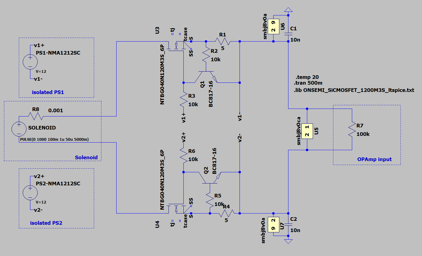
Input protection is a very challanging part of the design, it. It is mandatory to keep the input resistances low as possible to limit thermal noise, while still protecting it from high voltage. Some days ago I getgot an idea from here, to use mosfetsMOSFETs and keep them fully open at normal conditions and close them when HV apears, I attaching the circuit.

Circuit:   

enter image description here

I am confused about how to drive the gate of these mosfets, whileMOSFETs. While isolated power supplies shouldcould be used, there is a concern about the switching frequency of these power supplies introducing harmonics that could couple to the input and add noise? I.

I have considered converters like:

On the PCB, there are two channels of the preamp circuit requiring 4xfour isolated switching DC-DC power supplies altogether. Each channel with an input and output 2nd order low-pass filter around 30 kHz. I plan to place the MOSFET protection before this filter on the chassis plane right next to the LEMO input connector. The

The output will be read by a high-end FPGA, enabling advanced digital filtering to eliminate known noise frequencies.

  1. Should I be concerned about potential noise from the four switching DC-DC converters? Is this frequnecy seperation would be enough as alone? The switching frequency will be more than 10x above my low-pass filter. Again, I would like to measure very low voltages in range of 100uV up to 30kHz, the gain is also very high which means the sensitivity will be also very high.

  2. With that FPGA a second order IIR notch filter could be used to filter out specified frequency band (LabView). Are my assumptations right and with synchronizing switching frequency of the converters, I can reduce and shrink the freq. range needed to filter out? Only in case if I really need to take care of that noise coming from converters.
    I a bit worry about using DCPA10512 integrated circuits, as they seem to have a design similar to the DCP02 Series, which has been on the market for 24 years.

    Should I be concerned about potential noise from the four switching DC-DC converters? Would this frequency seperation be enough alone? The switching frequency will be more than ten times my low-pass filter. Again, I would like to measure very low voltages in range of 100uV up to 30kHz, the gain is also very high which means the sensitivity will be also very high.
  3. Also looking for alternative solutions, avoiding using switching power supllies. The MOSFET would only need to turn off a few times per day during an experiment, requiring only 1-2 mA for a few milliseconds during switching off, with almost zero consumption otherwise. Is there any simple solution for providing here isolated "charge" for the gate?

    With that FPGA, a second order IIR notch filter could be used to filter out specified frequency band (LabView.) Are my assumptations right and with synchronizing switching frequency of the converters, I can reduce and shrink the freq. range needed to filter out? Only in case if I really need to take care of that noise coming from converters.

I a bit worry about using DCPA10512 integrated circuits as they seem to have a design similar to the DCP02 series, which has been on the market for 24 years.

  1. Also looking for alternative solutions, avoiding using switching power supllies. The MOSFET would only need to turn off a few times per day during an experiment, requiring only 1-2 mA for a few milliseconds during switching off, with almost zero consumption otherwise. Is there any simple solution for providing here isolated "charge" for the gate?

Could DC-DC Isolated Power Supply Switching Noise Harm the Input of an Instrumentation Preamplifier

I looking for a noisless protection against 100ms pulse of 1kV of an input of ultralow noise instrumentation preamplifier (8x AD8428 connected in paralell, fixed gain of x2000) to measure very low voltages around 100uV up to 30 kHz of bandwidth.

Input protection is a very challanging part of the design, it is mandatory to keep the input resistances low as possible to limit thermal noise, while still protecting it from high voltage. Some days ago I get an idea from here, to use mosfets and keep them fully open at normal conditions and close them when HV apears, I attaching the circuit:  enter image description here

I am confused about how to drive the gate of these mosfets, while isolated power supplies should be used, there is a concern about the switching frequency of these power supplies introducing harmonics that could couple to the input and add noise? I have considered converters like:

On the PCB, there are two channels of the preamp circuit requiring 4x isolated switching DC-DC power supplies altogether. Each channel with an input and output 2nd order low-pass filter around 30 kHz. I plan to place the MOSFET protection before this filter on the chassis plane right next to the LEMO input connector. The output will be read by a high-end FPGA, enabling advanced digital filtering to eliminate known noise frequencies.

  1. Should I be concerned about potential noise from the four switching DC-DC converters? Is this frequnecy seperation would be enough as alone? The switching frequency will be more than 10x above my low-pass filter. Again, I would like to measure very low voltages in range of 100uV up to 30kHz, the gain is also very high which means the sensitivity will be also very high.

  2. With that FPGA a second order IIR notch filter could be used to filter out specified frequency band (LabView). Are my assumptations right and with synchronizing switching frequency of the converters, I can reduce and shrink the freq. range needed to filter out? Only in case if I really need to take care of that noise coming from converters.
    I a bit worry about using DCPA10512 integrated circuits, as they seem to have a design similar to the DCP02 Series, which has been on the market for 24 years.

  3. Also looking for alternative solutions, avoiding using switching power supllies. The MOSFET would only need to turn off a few times per day during an experiment, requiring only 1-2 mA for a few milliseconds during switching off, with almost zero consumption otherwise. Is there any simple solution for providing here isolated "charge" for the gate?

Could DC-DC isolated power supply switching noise harm the input of an instrumentation preamplifier?

I am looking for a noiseless protection against 100ms pulse of 1kV of an input of ultralow noise instrumentation preamplifier (eight AD8428 connected in parallel, fixed gain of 2000) to measure very low voltages around 100uV up to 30 kHz of bandwidth.

Input protection is a very challanging part of the design. It is mandatory to keep the input resistances low as possible to limit thermal noise, while still protecting it from high voltage. Some days ago I got an idea from here, to use MOSFETs and keep them fully open at normal conditions and close them when HV apears.

Circuit: 

enter image description here

I am confused about how to drive the gate of these MOSFETs. While isolated power supplies could be used, there is a concern about the switching frequency of these power supplies introducing harmonics that could couple to the input and add noise.

I have considered converters like:

On the PCB, there are two channels of the preamp circuit requiring four isolated switching DC-DC power supplies altogether. Each channel with an input and output 2nd order low-pass filter around 30 kHz. I plan to place the MOSFET protection before this filter on the chassis plane right next to the LEMO input connector.

The output will be read by a high-end FPGA, enabling advanced digital filtering to eliminate known noise frequencies.

  1. Should I be concerned about potential noise from the four switching DC-DC converters? Would this frequency seperation be enough alone? The switching frequency will be more than ten times my low-pass filter. Again, I would like to measure very low voltages in range of 100uV up to 30kHz, the gain is also very high which means the sensitivity will be also very high.
  2. With that FPGA, a second order IIR notch filter could be used to filter out specified frequency band (LabView.) Are my assumptations right and with synchronizing switching frequency of the converters, I can reduce and shrink the freq. range needed to filter out? Only in case if I really need to take care of that noise coming from converters.

I a bit worry about using DCPA10512 integrated circuits as they seem to have a design similar to the DCP02 series, which has been on the market for 24 years.

  1. Also looking for alternative solutions, avoiding using switching power supllies. The MOSFET would only need to turn off a few times per day during an experiment, requiring only 1-2 mA for a few milliseconds during switching off, with almost zero consumption otherwise. Is there any simple solution for providing here isolated "charge" for the gate?
deleted 2 characters in body
Source Link
NNN123
  • 103
  • 7

I looking for a noisless protection against 100ms pulse of 1kV of an input of ultralow noise instrumentation preamplifier (8x AD8428 connected in paralell, fixed gain of x2000) to measure very low voltages around 100uV up to 30 kHz of bandwidth.

Input protection is a very challanging part of the design, it is mandatory to keep the input resistances low as possible to limit thermal noise, while still protecting it from high voltage. Some days ago I get an idea from here, to use mosfets and keep them fully open at normal conditions and close them when HV apears, I attaching the circuit: enter image description here

I am confused about how to drive the gate of these mosfets, while isolated power supplies should be used, there is a concern about the switching frequency of these power supplies introducing harmonics that could couple to the input and add noise? I have considered converters like:

  • TRV 1-1513M using 220 - 380 kHz
  • DCPA10512 using 750 - 1000 kHz

Both using fixed frequency PWM mode over PFM mode, to prevent moving frequency and moving harmonics. The switching frequency of DCPA10512 moreover can be synchronized.

On the PCB, there are two channels of the preamp circuit, each requiring 4x isolated switching DC-DC power supplies altogether. Each channel with an input and output 2nd order low-pass filter around 30 kHz. I plan to place the MOSFET protection before thethis filter on the chassis plane right next to the LEMO input connector, requiring 4x isolated switching DC-DC power supplies for the two channels. The output will be read by a high-end FPGA, enabling advanced digital filtering to eliminate known noise frequencies.

My questions:

  1. Should I be concerned about potential noise from the four switching DC-DC converters? Is this frequnecy seperation would be enough as alone? The switching frequency will be more than 10x above my low-pass filter. Again, I would like to measure very low voltages in range of 100uV up to 30kHz, the gain is also very high which means the sensitivity will be also very high.

  2. With that FPGA a second order IIR notch filter could be used to filter out specified frequency band (LabView). Are my assumptations right and with synchronizing switching frequency of the converters, I can reduce and shrink the freq. range needed to filter out? Only in case if I really need to take care of that noise coming from converters.
    I a bit worry about using DCPA10512 integrated circuits, as they seem to have a design similar to the DCP02 Series, which has been on the market for 24 years.

  3. Also looking for alternative solutions, avoiding using switching power supllies. The MOSFET would only need to turn off a few times per day during an experiment, requiring only 1-2 mA for a few milliseconds during switching off, with almost zero consumption otherwise. Is there any simple solution for providing here isolated "charge" for the gate?

I looking for a noisless protection against 100ms pulse of 1kV of an input of ultralow noise instrumentation preamplifier (8x AD8428 connected in paralell, fixed gain of x2000) to measure very low voltages around 100uV up to 30 kHz of bandwidth.

Input protection is a very challanging part of the design, it is mandatory to keep the input resistances low as possible to limit thermal noise, while still protecting it from high voltage. Some days ago I get an idea from here, to use mosfets and keep them fully open at normal conditions and close them when HV apears, I attaching the circuit: enter image description here

I am confused about how to drive the gate of these mosfets, while isolated power supplies should be used, there is a concern about the switching frequency of these power supplies introducing harmonics that could couple to the input and add noise? I have considered converters like:

  • TRV 1-1513M using 220 - 380 kHz
  • DCPA10512 using 750 - 1000 kHz

Both using fixed frequency PWM mode over PFM mode, to prevent moving frequency and moving harmonics. The switching frequency of DCPA10512 moreover can be synchronized.

On the PCB, there are two channels of the preamp circuit, each with an input and output 2nd order low-pass filter around 30 kHz. I plan to place the MOSFET protection before the filter on the chassis plane right next to the LEMO input connector, requiring 4x isolated switching DC-DC power supplies for the two channels. The output will be read by a high-end FPGA, enabling advanced digital filtering to eliminate known noise frequencies.

My questions:

  1. Should I be concerned about potential noise from the four switching DC-DC converters? Is this frequnecy seperation would be enough as alone? The switching frequency will be more than 10x above my low-pass filter. Again, I would like to measure very low voltages in range of 100uV, the gain is also very high which means the sensitivity will be also very high.

  2. With that FPGA a second order IIR notch filter could be used to filter out specified frequency band (LabView). Are my assumptations right and with synchronizing switching frequency of the converters, I can reduce and shrink the freq. range needed to filter out? Only in case if I really need to take care of that noise coming from converters.
    I a bit worry about using DCPA10512 integrated circuits, as they seem to have a design similar to the DCP02 Series, which has been on the market for 24 years.

  3. Also looking for alternative solutions, avoiding using switching power supllies. The MOSFET would only need to turn off a few times per day during an experiment, requiring only 1-2 mA for a few milliseconds during switching off, with almost zero consumption otherwise. Is there any simple solution for providing here isolated "charge" for the gate?

I looking for a noisless protection against 100ms pulse of 1kV of an input of ultralow noise instrumentation preamplifier (8x AD8428 connected in paralell, fixed gain of x2000) to measure very low voltages around 100uV up to 30 kHz of bandwidth.

Input protection is a very challanging part of the design, it is mandatory to keep the input resistances low as possible to limit thermal noise, while still protecting it from high voltage. Some days ago I get an idea from here, to use mosfets and keep them fully open at normal conditions and close them when HV apears, I attaching the circuit: enter image description here

I am confused about how to drive the gate of these mosfets, while isolated power supplies should be used, there is a concern about the switching frequency of these power supplies introducing harmonics that could couple to the input and add noise? I have considered converters like:

  • TRV 1-1513M using 220 - 380 kHz
  • DCPA10512 using 750 - 1000 kHz

Both using fixed frequency PWM mode over PFM mode, to prevent moving frequency and moving harmonics. The switching frequency of DCPA10512 moreover can be synchronized.

On the PCB, there are two channels of the preamp circuit requiring 4x isolated switching DC-DC power supplies altogether. Each channel with an input and output 2nd order low-pass filter around 30 kHz. I plan to place the MOSFET protection before this filter on the chassis plane right next to the LEMO input connector. The output will be read by a high-end FPGA, enabling advanced digital filtering to eliminate known noise frequencies.

My questions:

  1. Should I be concerned about potential noise from the four switching DC-DC converters? Is this frequnecy seperation would be enough as alone? The switching frequency will be more than 10x above my low-pass filter. Again, I would like to measure very low voltages in range of 100uV up to 30kHz, the gain is also very high which means the sensitivity will be also very high.

  2. With that FPGA a second order IIR notch filter could be used to filter out specified frequency band (LabView). Are my assumptations right and with synchronizing switching frequency of the converters, I can reduce and shrink the freq. range needed to filter out? Only in case if I really need to take care of that noise coming from converters.
    I a bit worry about using DCPA10512 integrated circuits, as they seem to have a design similar to the DCP02 Series, which has been on the market for 24 years.

  3. Also looking for alternative solutions, avoiding using switching power supllies. The MOSFET would only need to turn off a few times per day during an experiment, requiring only 1-2 mA for a few milliseconds during switching off, with almost zero consumption otherwise. Is there any simple solution for providing here isolated "charge" for the gate?

Source Link
NNN123
  • 103
  • 7

Could DC-DC Isolated Power Supply Switching Noise Harm the Input of an Instrumentation Preamplifier

I looking for a noisless protection against 100ms pulse of 1kV of an input of ultralow noise instrumentation preamplifier (8x AD8428 connected in paralell, fixed gain of x2000) to measure very low voltages around 100uV up to 30 kHz of bandwidth.

Input protection is a very challanging part of the design, it is mandatory to keep the input resistances low as possible to limit thermal noise, while still protecting it from high voltage. Some days ago I get an idea from here, to use mosfets and keep them fully open at normal conditions and close them when HV apears, I attaching the circuit: enter image description here

I am confused about how to drive the gate of these mosfets, while isolated power supplies should be used, there is a concern about the switching frequency of these power supplies introducing harmonics that could couple to the input and add noise? I have considered converters like:

  • TRV 1-1513M using 220 - 380 kHz
  • DCPA10512 using 750 - 1000 kHz

Both using fixed frequency PWM mode over PFM mode, to prevent moving frequency and moving harmonics. The switching frequency of DCPA10512 moreover can be synchronized.

On the PCB, there are two channels of the preamp circuit, each with an input and output 2nd order low-pass filter around 30 kHz. I plan to place the MOSFET protection before the filter on the chassis plane right next to the LEMO input connector, requiring 4x isolated switching DC-DC power supplies for the two channels. The output will be read by a high-end FPGA, enabling advanced digital filtering to eliminate known noise frequencies.

My questions:

  1. Should I be concerned about potential noise from the four switching DC-DC converters? Is this frequnecy seperation would be enough as alone? The switching frequency will be more than 10x above my low-pass filter. Again, I would like to measure very low voltages in range of 100uV, the gain is also very high which means the sensitivity will be also very high.

  2. With that FPGA a second order IIR notch filter could be used to filter out specified frequency band (LabView). Are my assumptations right and with synchronizing switching frequency of the converters, I can reduce and shrink the freq. range needed to filter out? Only in case if I really need to take care of that noise coming from converters.
    I a bit worry about using DCPA10512 integrated circuits, as they seem to have a design similar to the DCP02 Series, which has been on the market for 24 years.

  3. Also looking for alternative solutions, avoiding using switching power supllies. The MOSFET would only need to turn off a few times per day during an experiment, requiring only 1-2 mA for a few milliseconds during switching off, with almost zero consumption otherwise. Is there any simple solution for providing here isolated "charge" for the gate?