Minor edit
Source Link
Circuit fantasist
  • 19.5k
  • 2
  • 23
  • 70

schematicschematic

simulate this circuitsimulate this circuit – Schematic created using CircuitLab

schematicschematic

simulate this circuitsimulate this circuit

schematicschematic

simulate this circuitsimulate this circuit
schematicschematic

simulate this circuitsimulate this circuit

schematicschematic

simulate this circuitsimulate this circuit
schematicschematic

simulate this circuitsimulate this circuit
schematicschematic

simulate this circuitsimulate this circuit
schematicschematic

simulate this circuitsimulate this circuit
schematicschematic

simulate this circuitsimulate this circuit
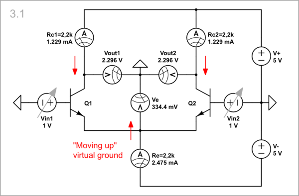
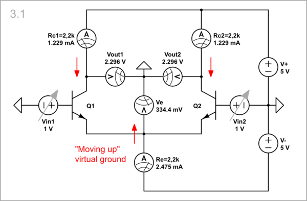
The result is the same as in the pure differential mode above - the output voltages change significantly because the midpoint between the emitters is moved but still "fixed"; it acts as a "shifted virtual ground".

Improvement

As can be seen from Schematics 3.1 and 3.2, the output voltages, although not much, still change when we change the two input voltages simultaneously (common mode). This is a problem because we usually use one of them as a single-ended output.

Increased Re and V-

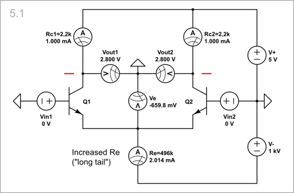
The straightforward solution invented a century ago was to simultaneously increase Re e.g. to 500 kΩ, and V- to -1000 V (although unrealistic); hence the name "long-tailed pair".

Vin1 = Vin2 = 0 V: Then the emitter and collector currents, and the collector voltages will be the same as in the initial Schematic 1.1.

schematic

simulate this circuit

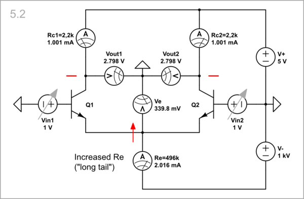
Vin1 = Vin2 = 1 V: But when we simultaneously increase both Vin1 and Vin2...

schematic

simulate this circuit

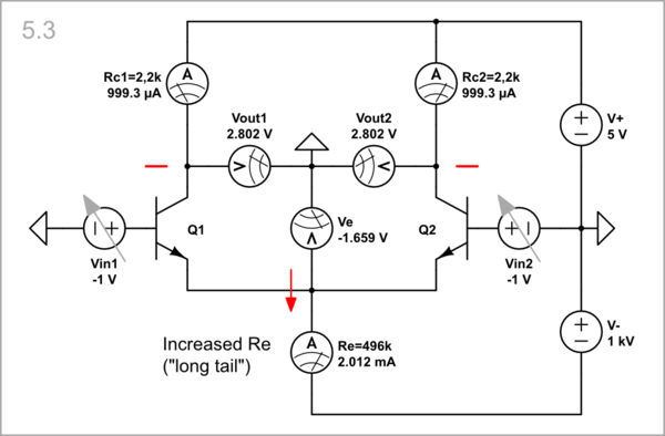
Vin1 = Vin2 = -1 V: ... or simultaneously decrease them...

schematic

simulate this circuit

... nothing will change. In other words, the common-mode input voltage gain is 0.

Dynamic Re

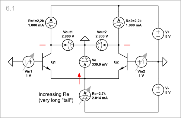
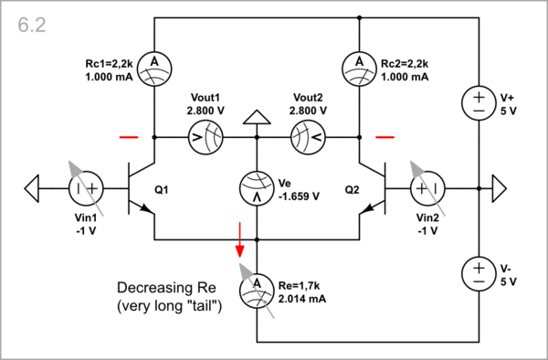
But later they thought that it was not reasonable to increase the voltage V- so much and came up with a smarter solution - to change Re simultaneously and in the same direction with both Vin... to make it dynamic. Let's simulate it by replacing the constant resistor Re with a variable one.

Vin1 = Vin2 = 1 V: Now, when the input voltages rise to 1 V, we increase Re to 2.7 kΩ...

schematic

simulate this circuit

Vin1 = Vin2 = -1 V: ... and when the input voltages drop to -1 V, we decrease Re to 1.7 kΩ.

schematic

simulate this circuit

The result is even better than above - absolutely nothing changes.

Emitter current source

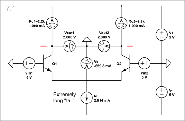
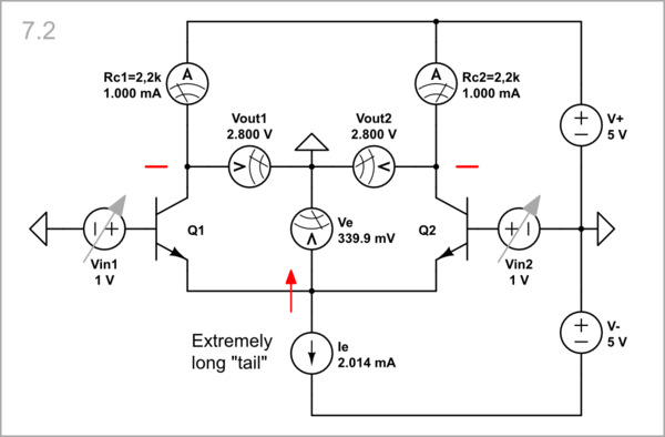
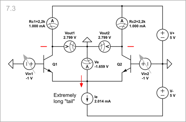
In fact what we have done above is what they call a "current source"; only it is manually controlled. Let's replace it with a standalone current source from the CircuitLab library and repeat the above experiments.

Vin1 = Vin2 = 0 V: Whether the input voltages are 0 V...

schematic

simulate this circuit

Vin1 = Vin2 = 1 V: ... or 1 V...

schematic

simulate this circuit

Vin1 = Vin2 = -1 V: ... or -1 V...

schematic

simulate this circuit

... the result is the same - no change.

Transistor current source

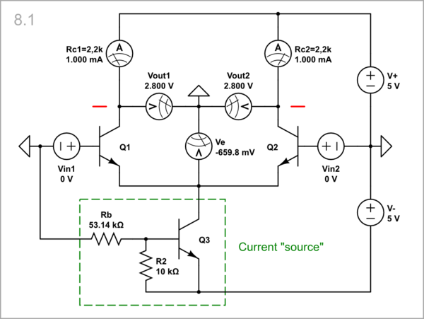
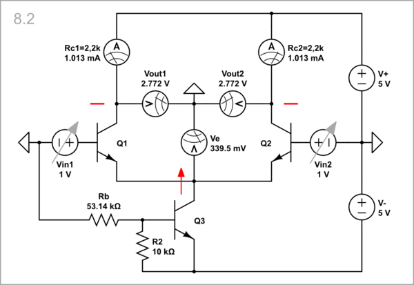
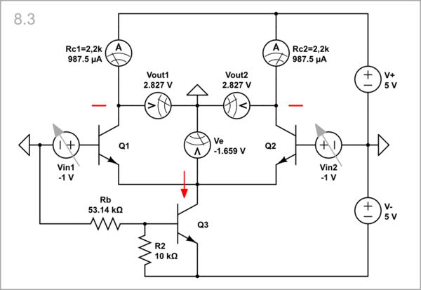
Let's finish this story about the famous long-tailed pair with a practical implementation of the emitter current source. We use the property of the transistor at a constant input (base-emitter) voltage to behave as a dynamic "resistor" that keeps its output (collector) current constant.

Vin1 = Vin2 = 0 V: Initially it has "resistance" 2.2 kΩ...

schematic

simulate this circuit

Vin1 = Vin2 = 1 V: ... then 2.7 kΩ...

schematic

simulate this circuit

... and finally 1.7 kΩ.

Vin1 = Vin2 = -1 V:

schematic

simulate this circuit

The result is almost the same - there is a small change (the transistor is real, though).

schematic

simulate this circuit – Schematic created using CircuitLab

schematic

simulate this circuit

schematic

simulate this circuit

schematic

simulate this circuit

schematic

simulate this circuit

schematic

simulate this circuit

schematic

simulate this circuit

schematic

simulate this circuit

schematic

simulate this circuit

The result is the same as in the pure differential mode above - the output voltages change significantly because the midpoint between the emitters is moved but still "fixed"; it acts as a "shifted virtual ground".

schematic

simulate this circuit – Schematic created using CircuitLab

schematic

simulate this circuit

schematic

simulate this circuit

schematic

simulate this circuit

schematic

simulate this circuit

schematic

simulate this circuit

schematic

simulate this circuit

schematic

simulate this circuit

schematic

simulate this circuit

The result is the same as in the pure differential mode above - the output voltages change significantly because the midpoint between the emitters is moved but still "fixed"; it acts as a "shifted virtual ground".

Improvement

As can be seen from Schematics 3.1 and 3.2, the output voltages, although not much, still change when we change the two input voltages simultaneously (common mode). This is a problem because we usually use one of them as a single-ended output.

Increased Re and V-

The straightforward solution invented a century ago was to simultaneously increase Re e.g. to 500 kΩ, and V- to -1000 V (although unrealistic); hence the name "long-tailed pair".

Vin1 = Vin2 = 0 V: Then the emitter and collector currents, and the collector voltages will be the same as in the initial Schematic 1.1.

schematic

simulate this circuit

Vin1 = Vin2 = 1 V: But when we simultaneously increase both Vin1 and Vin2...

schematic

simulate this circuit

Vin1 = Vin2 = -1 V: ... or simultaneously decrease them...

schematic

simulate this circuit

... nothing will change. In other words, the common-mode input voltage gain is 0.

Dynamic Re

But later they thought that it was not reasonable to increase the voltage V- so much and came up with a smarter solution - to change Re simultaneously and in the same direction with both Vin... to make it dynamic. Let's simulate it by replacing the constant resistor Re with a variable one.

Vin1 = Vin2 = 1 V: Now, when the input voltages rise to 1 V, we increase Re to 2.7 kΩ...

schematic

simulate this circuit

Vin1 = Vin2 = -1 V: ... and when the input voltages drop to -1 V, we decrease Re to 1.7 kΩ.

schematic

simulate this circuit

The result is even better than above - absolutely nothing changes.

Emitter current source

In fact what we have done above is what they call a "current source"; only it is manually controlled. Let's replace it with a standalone current source from the CircuitLab library and repeat the above experiments.

Vin1 = Vin2 = 0 V: Whether the input voltages are 0 V...

schematic

simulate this circuit

Vin1 = Vin2 = 1 V: ... or 1 V...

schematic

simulate this circuit

Vin1 = Vin2 = -1 V: ... or -1 V...

schematic

simulate this circuit

... the result is the same - no change.

Transistor current source

Let's finish this story about the famous long-tailed pair with a practical implementation of the emitter current source. We use the property of the transistor at a constant input (base-emitter) voltage to behave as a dynamic "resistor" that keeps its output (collector) current constant.

Vin1 = Vin2 = 0 V: Initially it has "resistance" 2.2 kΩ...

schematic

simulate this circuit

Vin1 = Vin2 = 1 V: ... then 2.7 kΩ...

schematic

simulate this circuit

... and finally 1.7 kΩ.

Vin1 = Vin2 = -1 V:

schematic

simulate this circuit

The result is almost the same - there is a small change (the transistor is real, though).

Added related link
Source Link
Circuit fantasist
  • 19.5k
  • 2
  • 23
  • 70

The result is the same as in the pure differential mode above - the output voltages change significantly because the midpoint between the emitters is moved but still "fixed"; it acts as a shifted"shifted virtual groundground".


See also my Codidact paper about the same circuit accompanied by real experiments.

The result is the same as in the pure differential mode above - the output voltages change significantly because the midpoint between the emitters is moved but still "fixed"; it acts as a shifted virtual ground.

The result is the same as in the pure differential mode above - the output voltages change significantly because the midpoint between the emitters is moved but still "fixed"; it acts as a "shifted virtual ground".


See also my Codidact paper about the same circuit accompanied by real experiments.

Added another consideration
Source Link
Circuit fantasist
  • 19.5k
  • 2
  • 23
  • 70

Basic idea

The differential pair (figuratively called "long-tailed pair" in the past) consists of two common-emitter stages with a common current source in the emitters. Depending on the mode of operation, they either cooperate (common mode) or oppose (differential mode). The output voltages reflect the "efforts" of the two transistors in this interaction - in the first case they are insignificant (small gain), and in the second significant (high gain). Usually one of the outputs is used which causes problems with the common-mode voltage.

Experimental arrangementsetup

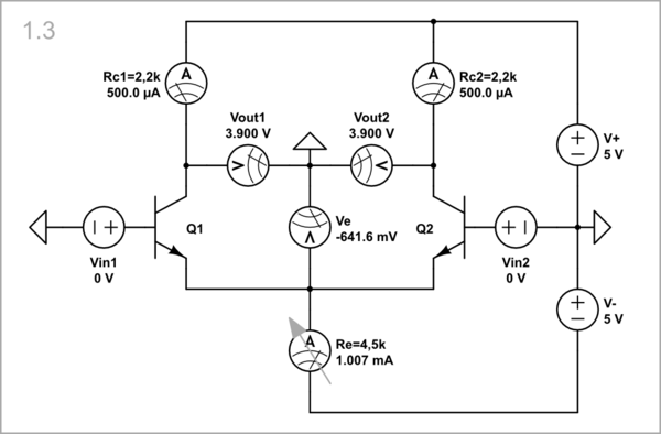
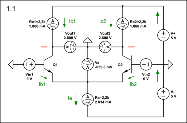
I have illustrated your arrangement (with corrected Ie = 2 mA) by a little unusual CircuitLab simulation consisting only of voltage sources and meters (see the schematics below). My idea was to visualize the most important electrical quantities without cluttering the schematic. For this purpose, I have presented the collector resistors as ammeters with an internal resistance of 2.2 kΩ, and the emitter resistor - through a voltmeter with an internal resistance of 2.2 kΩ. Simply put, think of them as "visualized resistors". The collector and emitter voltages are visualized with ordinary (perfect) voltmeters. Note that their "black probes" are connected to ground (the midpoint of the power supply). The current directions are represented by arrows in green, and the voltage-change directions by arrows in red.

I suggest revealing the ideas behind this famous circuit (figuratively called "long-tailed pair" in the past) by doing a number of step-by-step experiments. The first of them (framed in black) is your circuit; the others (framed in pale gray) explore its operation modes.

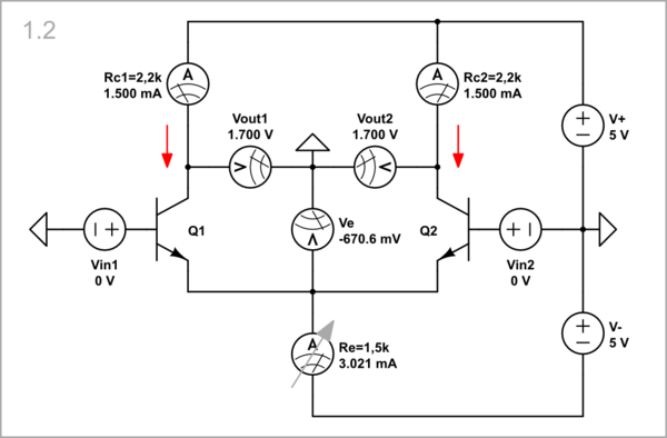
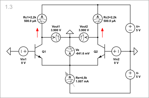
First we need to set the "initial state" of the circuit, or as it is commonly said, "establish the quiescent operating point". This means, at zero input voltages, adjust the emitter resistance Re so that its output currents and voltages are in the middle of the output range. This basically applies to any amplifier, but here it is a little more complicated because we have two types of signals - common-mode and differential-mode.

Ic1 = Ic2 = 1 mA: Assuming that at the common mode Vout will vary from -1 V to 1 V, we can agree with your current values of 1mA.

schematicschematic

simulate this circuitsimulate this circuit – Schematic created using CircuitLab
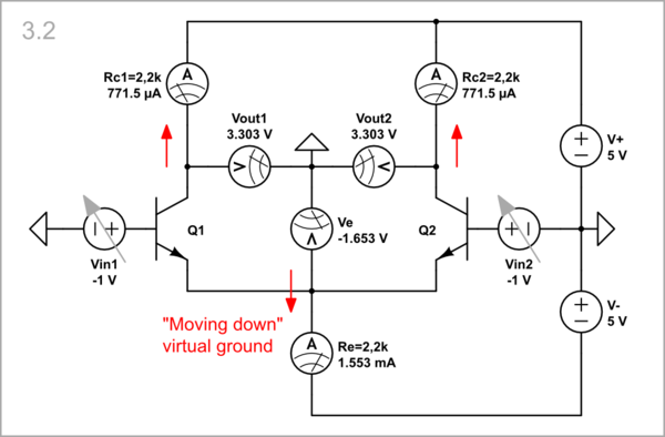
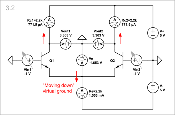
Ic1 = Ic2 = 1.5 mA: Now let's experiment a bit by first setting a higher current (less Re)...

schematicschematic

simulate this circuitsimulate this circuit
Ic1 = Ic2 = 0.5 mA: ... and then a lower current value (higher Re).

schematicschematic

simulate this circuitsimulate this circuit
Operation: The mechanism of this biasing is as follows. When we change Re with the purpose to change the emitter and accordingly the collector currents, the transistors react to this intervention by changing their collector currents so that to make their sum equal to the emitter current.

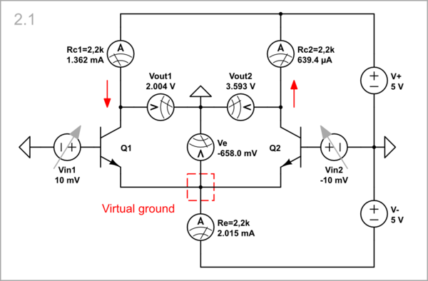
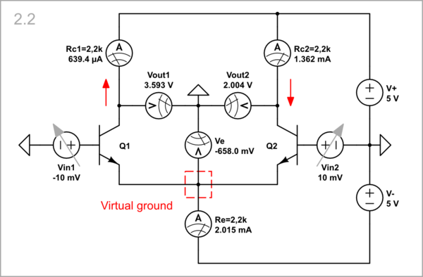
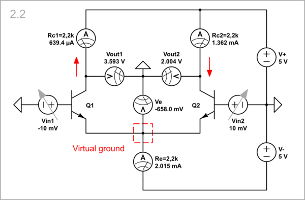
If we change (even slightly) the input voltages in opposite directions...

Vin1 = 10 mV, Vin2 = -10 mV: ... one way...

schematicschematic

simulate this circuitsimulate this circuit
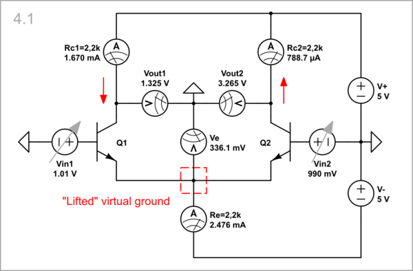
Vin1 = -10 mV, Vin2 = 10 mV: ... or the other...

schematicschematic

simulate this circuitsimulate this circuit
... the output voltages change significantly in opposite directions because the midpoint between the emitters is "fixed"; it acts as a virtual ground.

But if we change (even significantly) the input voltages in the same direction...

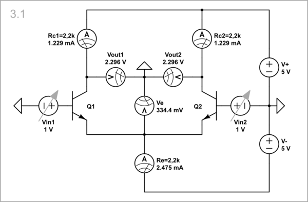
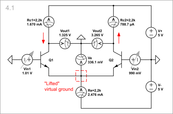
Vin1 = Vin2 = 1 V: ... e.g. by "lifting"...

schematicschematic

simulate this circuitsimulate this circuit
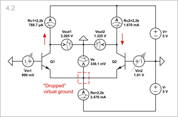
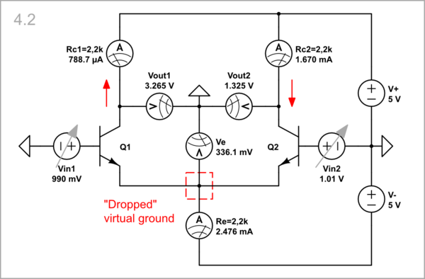
Vin1 = Vin2 = -1 V: ... or "dropping" both...

schematicschematic

simulate this circuitsimulate this circuit

... the output voltages change slightly because the emitter midpoint "moves" in the same direction with the input voltages.

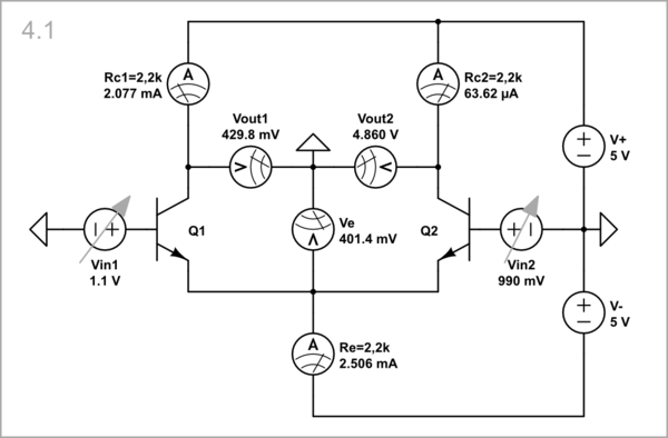
Normally, the input voltages are varied differentially against some common-mode voltage. Let's try it by first "lifting" the input voltages by 1 V, and then differentially change them by only 10 mV...

Vin1 = 1.101 V, Vin2 = 0.99 V: ... in one...

schematicschematic

simulate this circuitsimulate this circuit

Vin1 = 0.99 V, Vin2 = 1.101 V: ... or the other direction.

schematicschematic

simulate this circuitsimulate this circuit

The result is the same as in the pure differential mode above - the output voltages change significantly because the midpoint between the emitters is moved but still "fixed"; it acts as a shifted virtual ground.

Experimental arrangement

I have illustrated your arrangement (with corrected Ie = 2 mA) by a little unusual CircuitLab simulation consisting only of voltage sources and meters (see the schematics below). My idea was to visualize the most important electrical quantities without cluttering the schematic. For this purpose, I have presented the collector resistors as ammeters with an internal resistance of 2.2 kΩ, and the emitter resistor - through a voltmeter with an internal resistance of 2.2 kΩ. Simply put, think of them as "visualized resistors". The collector and emitter voltages are visualized with ordinary (perfect) voltmeters. Note that their "black probes" are connected to ground (the midpoint of the power supply).

I suggest revealing the ideas behind this famous circuit (figuratively called "long-tailed pair" in the past) by doing a number of step-by-step experiments. The first of them (framed in black) is your circuit; the others (framed in pale gray) explore its operation modes.

Ic1 = Ic2 = 1 mA

schematic

simulate this circuit – Schematic created using CircuitLab

Ic1 = Ic2 = 1.5 mA

schematic

simulate this circuit

Ic1 = Ic2 = 0.5 mA

schematic

simulate this circuit

Vin1 = 10 mV, Vin2 = -10 mV

schematic

simulate this circuit

Vin1 = -10 mV, Vin2 = 10 mV

schematic

simulate this circuit

Vin1 = Vin2 = 1 V

schematic

simulate this circuit

Vin1 = Vin2 = -1 V

schematic

simulate this circuit

Vin1 = 1.1 V, Vin2 = 0.99 V

schematic

simulate this circuit

Vin1 = 0.99 V, Vin2 = 1.1 V

schematic

simulate this circuit

Basic idea

The differential pair (figuratively called "long-tailed pair" in the past) consists of two common-emitter stages with a common current source in the emitters. Depending on the mode of operation, they either cooperate (common mode) or oppose (differential mode). The output voltages reflect the "efforts" of the two transistors in this interaction - in the first case they are insignificant (small gain), and in the second significant (high gain). Usually one of the outputs is used which causes problems with the common-mode voltage.

Experimental setup

I have illustrated your arrangement (with corrected Ie = 2 mA) by a little unusual CircuitLab simulation consisting only of voltage sources and meters (see the schematics below). My idea was to visualize the most important electrical quantities without cluttering the schematic. For this purpose, I have presented the collector resistors as ammeters with an internal resistance of 2.2 kΩ, and the emitter resistor - through a voltmeter with an internal resistance of 2.2 kΩ. Simply put, think of them as "visualized resistors". The collector and emitter voltages are visualized with ordinary (perfect) voltmeters. Note that their "black probes" are connected to ground (the midpoint of the power supply). The current directions are represented by arrows in green, and the voltage-change directions by arrows in red.

I suggest revealing the ideas behind this famous circuit by doing a number of step-by-step experiments. The first of them (framed in black) is your circuit; the others (framed in pale gray) explore its operation modes.

First we need to set the "initial state" of the circuit, or as it is commonly said, "establish the quiescent operating point". This means, at zero input voltages, adjust the emitter resistance Re so that its output currents and voltages are in the middle of the output range. This basically applies to any amplifier, but here it is a little more complicated because we have two types of signals - common-mode and differential-mode.

Ic1 = Ic2 = 1 mA: Assuming that at the common mode Vout will vary from -1 V to 1 V, we can agree with your current values of 1mA.

schematic

simulate this circuit – Schematic created using CircuitLab

Ic1 = Ic2 = 1.5 mA: Now let's experiment a bit by first setting a higher current (less Re)...

schematic

simulate this circuit

Ic1 = Ic2 = 0.5 mA: ... and then a lower current value (higher Re).

schematic

simulate this circuit

Operation: The mechanism of this biasing is as follows. When we change Re with the purpose to change the emitter and accordingly the collector currents, the transistors react to this intervention by changing their collector currents so that to make their sum equal to the emitter current.

If we change (even slightly) the input voltages in opposite directions...

Vin1 = 10 mV, Vin2 = -10 mV: ... one way...

schematic

simulate this circuit

Vin1 = -10 mV, Vin2 = 10 mV: ... or the other...

schematic

simulate this circuit

... the output voltages change significantly in opposite directions because the midpoint between the emitters is "fixed"; it acts as a virtual ground.

But if we change (even significantly) the input voltages in the same direction...

Vin1 = Vin2 = 1 V: ... e.g. by "lifting"...

schematic

simulate this circuit

Vin1 = Vin2 = -1 V: ... or "dropping" both...

schematic

simulate this circuit

... the output voltages change slightly because the emitter midpoint "moves" in the same direction with the input voltages.

Normally, the input voltages are varied differentially against some common-mode voltage. Let's try it by first "lifting" the input voltages by 1 V, and then differentially change them by only 10 mV...

Vin1 = 1.01 V, Vin2 = 0.99 V: ... in one...

schematic

simulate this circuit

Vin1 = 0.99 V, Vin2 = 1.01 V: ... or the other direction.

schematic

simulate this circuit

The result is the same as in the pure differential mode above - the output voltages change significantly because the midpoint between the emitters is moved but still "fixed"; it acts as a shifted virtual ground.

Corrected arrow in Schematic 3.2
Source Link
Circuit fantasist
  • 19.5k
  • 2
  • 23
  • 70
Loading
Corrected schematics
Source Link
Circuit fantasist
  • 19.5k
  • 2
  • 23
  • 70
Loading
Minor edit
Source Link
Circuit fantasist
  • 19.5k
  • 2
  • 23
  • 70
Loading
Added OP's citation
Source Link
Circuit fantasist
  • 19.5k
  • 2
  • 23
  • 70
Loading
Source Link
Circuit fantasist
  • 19.5k
  • 2
  • 23
  • 70
Loading