What is the right design rules from JLCPCB? When I look at the electrical clearance from JLCPCB, I find:

  • Via to Via (Same net labels): 0.254mm
  • Hole to hole (Different net labels): 0.5mm
  • Pad to pad (Different net labels): 0.127mm
  • Pad to Pad with hole (Different net labels): 0.5mm
  • Via to track: 0.254 mm
  • Plated Hole to track: 0.33mm
  • Non Plated Hole to track: 0.254mm
  • Pad to track: 0.2mm
  • Minimum spacning: 0.09mm (4-6 layers)

https://jlcpcb.com/capabilities/pcb-capabilities

Question:

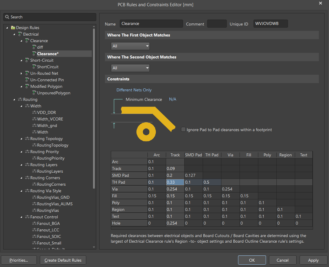
Is thisAre these the correct settings of the design rules?

enter image description here

Issue:

The issue is that it seems like a regular BGA footprint cannot even be produced by JLCPCB with those desgindesign rules. I have downloaded a sample CAD model from STMicroelectronics and it seems that all the rules from that model, violates violate the JLCPCB rules. Is that correct?

What is the right design rules from JLCPCB? When I look at the electrical clearance from JLCPCB, I find:

  • Via to Via (Same net labels): 0.254mm
  • Hole to hole (Different net labels): 0.5mm
  • Pad to pad (Different net labels): 0.127mm
  • Pad to Pad with hole (Different net labels): 0.5mm
  • Via to track: 0.254 mm
  • Plated Hole to track: 0.33mm
  • Non Plated Hole to track: 0.254mm
  • Pad to track: 0.2mm
  • Minimum spacning: 0.09mm (4-6 layers)

https://jlcpcb.com/capabilities/pcb-capabilities

Question:

Is this the correct settings of the design rules?

enter image description here

Issue:

The issue is that it seems like a regular BGA footprint cannot even be produced by JLCPCB with those desgin rules. I have downloaded a sample CAD model from STMicroelectronics and it seems that all the rules from that model, violates the JLCPCB rules. Is that correct?

What is the right design rules from JLCPCB? When I look at the electrical clearance from JLCPCB, I find:

  • Via to Via (Same net labels): 0.254mm
  • Hole to hole (Different net labels): 0.5mm
  • Pad to pad (Different net labels): 0.127mm
  • Pad to Pad with hole (Different net labels): 0.5mm
  • Via to track: 0.254 mm
  • Plated Hole to track: 0.33mm
  • Non Plated Hole to track: 0.254mm
  • Pad to track: 0.2mm
  • Minimum spacning: 0.09mm (4-6 layers)

https://jlcpcb.com/capabilities/pcb-capabilities

Question:

Are these the correct settings of the design rules?

enter image description here

Issue:

The issue is that it seems like a regular BGA footprint cannot even be produced by JLCPCB with those design rules. I have downloaded a sample CAD model from STMicroelectronics and it seems that all the rules from that model violate the JLCPCB rules. Is that correct?

Source Link
euraad
  • 1.4k
  • 17
  • 42

JLPCB Design Rules for Altium CircuitMaker

What is the right design rules from JLCPCB? When I look at the electrical clearance from JLCPCB, I find:

  • Via to Via (Same net labels): 0.254mm
  • Hole to hole (Different net labels): 0.5mm
  • Pad to pad (Different net labels): 0.127mm
  • Pad to Pad with hole (Different net labels): 0.5mm
  • Via to track: 0.254 mm
  • Plated Hole to track: 0.33mm
  • Non Plated Hole to track: 0.254mm
  • Pad to track: 0.2mm
  • Minimum spacning: 0.09mm (4-6 layers)

https://jlcpcb.com/capabilities/pcb-capabilities

Question:

Is this the correct settings of the design rules?

enter image description here

Issue:

The issue is that it seems like a regular BGA footprint cannot even be produced by JLCPCB with those desgin rules. I have downloaded a sample CAD model from STMicroelectronics and it seems that all the rules from that model, violates the JLCPCB rules. Is that correct?