1
\$\begingroup\$

I have a bottom gate TFT transistor:

  • W/l=320um
  • Substrate: corning glass
  • Gate: 60nm Molibdenum
  • Dielectric: 350 nm Ta2O5
  • Semiconductor: 30nm IGZO
  • S-D: Molibdenum 60nm

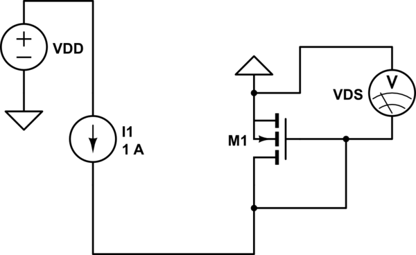
It is wired like in current mirror setup https://en.wikipedia.org/wiki/Current_mirror#Basic_MOSFET_current_mirror :

schematic

simulate this circuit – Schematic created using CircuitLab

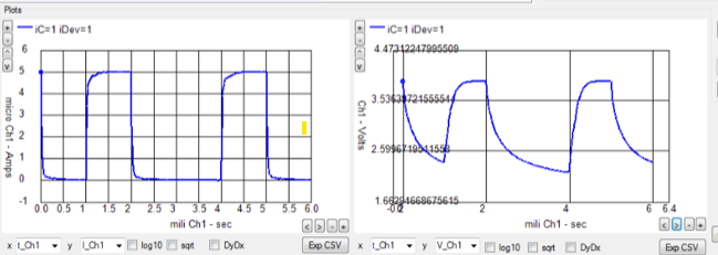
I am forcing pulses of current IDS and registering VGS=VDS This is what it looks like on the SMU:

  • Plot 1: CH1 IDS VS time
  • Plot 2: Ch1 VGS vs time

Plots

I want to wire a second transistor in the same way, get a recording VGS2 and then find the difference VGS1-VGS2.

The application

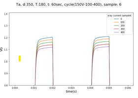
I am using the TFT to detect ionizing radiation: The X-ray radiation creates electron-hole pairs in the dielectric, which then affects the VGS recorded for a fixed ISD

Here is a plot showing how the VGS curve changes with the radiation exposure:

VGS vs Time

EDIT-from remices2 answer

Does the circuit in the answer of remicles2 work? Since it has only gotten down votes for now, but I think because it wasn't using my original circuit (which I edited now since I think it was my circuit that was wrong.)

\$\endgroup\$
16
  • \$\begingroup\$ This is quite broad, I suggest you study circuits with transistors and figure out how they work. Also "TFT transistors" are quite uncommon unless they are in an LCD. \$\endgroup\$ Commented Oct 16, 2019 at 12:15
  • 2
    \$\begingroup\$ TFT is "thin film transistor" typically used in LCD displays with transistors at each pixel position. The materials used to produce the MOSFETs in displays are transparent so that light can pass through. It is possible that @leoelectrics is trying to work with some other TFT's that are designed for some other application. It would be suggested that they describe more what the goal is. \$\endgroup\$ Commented Oct 16, 2019 at 13:17
  • 1
    \$\begingroup\$ @ElliotAlderson The experiment has already been done, we passed dc current and read VGS, those plots are from real data. Maybe I am still missing something in my circuit drawing \$\endgroup\$
    – Leo
    Commented Oct 16, 2019 at 18:35
  • 1
    \$\begingroup\$ Your schematic has no ground reference. Exactly how are you forcing current into the Drains, and how did you measure the Gate voltage on a single FET? \$\endgroup\$ Commented Oct 16, 2019 at 19:46
  • 1
    \$\begingroup\$ @ElliotAlderson, you can indeed run a MOSFET "backwards" and get a \$V_{GS}\$ from a fixed drain current. That's the essence of building a MOSFET current mirror: en.wikipedia.org/wiki/… \$\endgroup\$
    – remcycles
    Commented Oct 16, 2019 at 21:57

1 Answer 1

0
\$\begingroup\$

A typical way of amplifying the difference between two voltages is with an op-amp configuration known as a "differential amplifier". A basic explanation is here: http://hyperphysics.phy-astr.gsu.edu/hbase/Electronic/opampvar6.html

More information can be found on Wikipedia or in a circuits textbook. https://en.wikipedia.org/wiki/Differential_amplifier

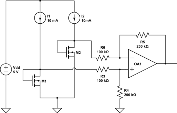
To add a differential amplifier to your circuit, I would first connect the source of each transistor to ground so they have the same \$V_S\$, the drain of each to its own identical current source, and connect the gates to the drain terminals (so that \$V_{GS}=V_{DS}\$, which will be determined by (1) the transistor geometry and materials, (2) the current source, and most importantly, (3) the radiation applied). This is called a "diode" connection, but I believe it is what you have already built and measured, or will at least will work the same way. I may be wrong here. From here, you can connect the two gates to the inputs of the differential amplifier. This schematic might be a good start (don't pay much attention to the component values, they're just placeholders):
schematic

simulate this circuit – Schematic created using CircuitLab

Two comments on your schematic diagrams, since they are unclear. First, your N-channel MOSFETs are mislabeled. You have swapped the source and drain terminals. Second, the wires in your schematic connect to an odd portion of the MOSFET symbol. See this picture for reference: https://en.wikipedia.org/wiki/MOSFET#/media/File:IGFET_N-Ch_Enh_Labelled.svg A schematic should only connect to the terminals of the MOSFET outside of the circled portion.

This is a cool application of a TFT, by the way.

EDIT:

The circuit I posted is very similar to a PTAT temperature sensor. Figure 4 at https://www.analog.com/en/analog-dialogue/articles/chip-to-monitor-environmental-conditions-on-motherboard.html# provides a clear example:
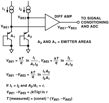
BJT PTAT temperature sensor

In a PTAT sensor, either the two current sources are different, or they are the same and the transistor geometries are different. This causes the two \$V_{BE}\$ voltages to respond differently with temperature changes. Measuring this voltage difference allows you to calculate the absolute temperature. If you can understand this principle, then you can see how your TFT radiation sensor works similarly. Now that I think about it, I would be concerned that your voltage measurements at a fixed radiation exposure will also change with temperature. You should confirm with environmental testing experiments.
\$\endgroup\$
17
  • 1
    \$\begingroup\$ @ElliotAlderson As I didn't setup the experiment, I probably remember it wrong, my bad. I think remicles2's solution with the drain and Gate shorted and the source set to ground is probably what they did. Can this circuit be simulated now with 2 different transistors to see that it actually is reading the VDS1-VDS2? \$\endgroup\$
    – Leo
    Commented Oct 17, 2019 at 5:21
  • 1
    \$\begingroup\$ @leoelectrics The voltmeter is connected to the correct terminals of the MOSFET, but the polarity is backwards. You want to measure between the Source and the Gate to get \$V_{GS}\$ which is equal to \$V_{DS}\$ in this circuit. In your updated schematic, the negative lead of the meter is connected to the Gate, but should be connected to the Source. That's not a huge problem, but you should know that a positive \$V_{GS}\$ will look like a negative voltage on that meter as it is currently connected. \$\endgroup\$
    – remcycles
    Commented Oct 17, 2019 at 17:30
  • 1
    \$\begingroup\$ @leoelectrics I don't have any experience using CircuitLab for simulation, but you should be able to change transistor properties and see a difference between VDS1 and VDS2. \$\endgroup\$
    – remcycles
    Commented Oct 17, 2019 at 17:37
  • 1
    \$\begingroup\$ Good catch. You are right, it is redundant. You can replace the ideal voltage source with a wire to get the same effect. I put it in there just because most real current sources need a source of power, but of course, an ideal current source is its own source of power. \$\endgroup\$
    – remcycles
    Commented Oct 18, 2019 at 17:29
  • 2
    \$\begingroup\$ An in-amp might be a better idea than a plain op-amp here, since that way you can avoid loading the circuit being measured. \$\endgroup\$
    – Hearth
    Commented Oct 18, 2019 at 19:52

Your Answer

By clicking “Post Your Answer”, you agree to our terms of service and acknowledge you have read our privacy policy.

Not the answer you're looking for? Browse other questions tagged or ask your own question.