1
\$\begingroup\$

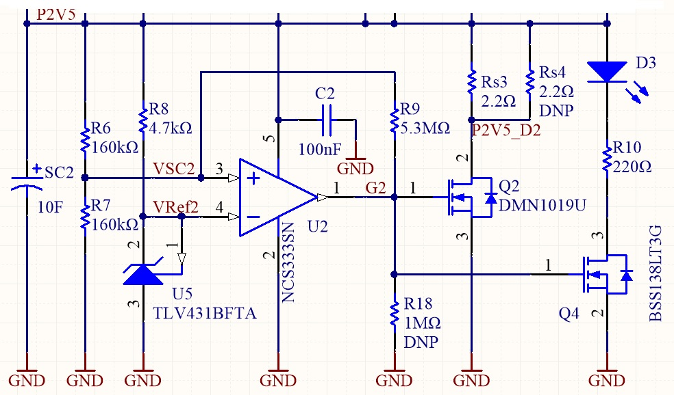
I have a Supercap voltage control circuit that is based on a On Semiconductor NCS333 Op Amp that's configured with hysteresis (using positive feedback) that drives two N-MOSFETs - one that is actually discharging Supercap when voltage goes over some pre-defined limit (~2.5V in my case) and another one to indicate that discharging is active now.

I've used DMN1019U MOSFET to discharge the Supercap as it can tolerate up to 10.7A of current with a very low \$\mathrm{V_{GS(th)}}\$ and \$\mathrm{R_{DS(on)}}\$, so it won't overheat at high currents. Current through MOSFET is limited by 2512-case resistor, \$\mathrm{R_S}\$, so most heat would be generated by resistor and not MOSFET.

When I'm using any resistor down to ~1.8Ohm - system works fine and correct, but if I want to increase discharge current by placing two 2.2Ohm resistors in parallel resulting in 1.1Ohm total resistance (for example) - output of Op Amp starts to oscillate and MOSFET starts to act as a variable resistor and heats up very quickly as its resistance becomes higher than \$\mathrm{R_S}\$ one.

I have tried to use snubber circuit for Op Amp, it helped a little bit, I was able to reduce \$\mathrm{R_S}\$ to ~1.5Ohm but if I go lower - oscillation starts again.

Is there any way to stabilize this circuit? I know that DMN1019U has a very high gate capacitance of 2588pF @ 10V, but I need to choose a MOSFET with lowest available resistance and \$\mathrm{V_{GS(th)}}\$ so power dissipation would be occurring in \$\mathrm{R_S}\$ rather than MOSFET.

enter image description here

\$\endgroup\$
11
  • \$\begingroup\$ Try putting some resistance in series with the MOSFET gate. It should be after the feedback network. Between feedback network and MOSFET gate. Try 10 Ohms and if that doesn't do it move up to 22, 47, 100, 220 or as high as you can go without slowing down the turn-on time to an unacceptable level. \$\endgroup\$
    – user57037
    Commented Feb 28, 2020 at 7:25
  • 1
    \$\begingroup\$ The TLV431 can be used as a comparator, against its internal voltage, why not use that directly? \$\endgroup\$
    – Neil_UK
    Commented Feb 28, 2020 at 8:20
  • 1
    \$\begingroup\$ Most op-amps do not like to drive capacitors. The idea of the resistor is to put it AFTER the feedback loop because if it is inside the feedback loop it will have no effect. I don't want to write a real answer and I can't post a picture in a comment. But break the wire right at the gate of Q2, and put the resistor right there at Q2. One side of the resistor is connected ONLY to Q2's gate. \$\endgroup\$
    – user57037
    Commented Feb 28, 2020 at 9:35
  • 1
    \$\begingroup\$ I would have tried to find a comparator to use in this application, since you are just trying to do rail-to-rail switching anyway. But I suspect you can get it to stop oscillating somehow if you keep at it. \$\endgroup\$
    – user57037
    Commented Feb 28, 2020 at 9:42
  • 1
    \$\begingroup\$ Something rated for 2.5 V and with rail-to-rail outputs. \$\endgroup\$
    – user57037
    Commented Feb 29, 2020 at 0:50

3 Answers 3

1
\$\begingroup\$

After a reading your question and having a quick look at the datasheets of the NCS333SN, I am sure that the problem is the heavy capacitive loading of the amplifier by the DMN1019. The two details motivate my belief

  1. The "Dynamic performance" parameter table at p. 6 states in each entry (apart from the slew rate SR entry) a value \$C_L=100\mathrm{pF}\$ for the load capacitance. This suggests that it is not advisable to increase too much beyond that limit the load capacitance.
  2. When you have a look at the "Typical characteristics" section, looking at figure 1, p. 7, you notice that the nice phase margin at \$f=f_T\$ of the amplifier is a more than respectable \$\phi_M\simeq 60^\circ\$ but again when the load capacitance is \$C_L=100\mathrm{pF}\$. And if look at figure 13, p. 9, you see that the small signal overshoot is over \$60\%\$ when \$C_L=1000\mathrm{pF}\$.

Since the typical gate capacitance of the DMN1019 is \$C_\mathrm{G}>2500\mathrm{pF}\$, we'll surely find troubles if we connect the OpAmp output directly to it: and even using a series gate resistor may not get you out of troubles, if this resistor is significantly lower respect to e.g. the standard load stated for the slew rate test, i.e. \$R_L=10\mathrm{k\Omega}\$, as you have noticed with your tests.

What could you do?

  1. Since you use the MOSFET as a means for discharging a supercap when the voltage across it starts to rise above the safe \$2.5\mathrm{V}\$ level, you do not need to be particularly fast in turning it on. Therefore you could try to put a \$10\mathrm{k\Omega}\$ gate resistor and see if the amplifier remains stable.
  2. Otherwise, if you desire to have nevertheless a quick response, you should try to find an optimal value for the gate resistor \$R_\mathrm{G}\$, by starting from \$R_\mathrm{G}=1000\Omega\$ and rising it until the circuit is stable for all desired resistor loads.

Final note

Following mkeith's comment above, I think is a very good idea to find a low voltage comparator and use it instead of the NCS333: despite their circuit topology can be (also very) similar, OpAmps and comparators cannot be used interchangeably without any care. Just to give some examples, devices like TLV3691 or NCS2200 could be a nice choice.

\$\endgroup\$
5
  • 1
    \$\begingroup\$ Thanks a lot for detailed description, I will try to stabilize this circuit using Rg! I thought it's other way around - Rg has to be small, that's why I was trying from 10Ohm up to 100Ohm and that didn't help. Also, I was putting Rg directly between output of Op Amp and gate of MOSFET while it has to be AFTER feedback network! \$\endgroup\$
    – Lt_Flash
    Commented Feb 29, 2020 at 6:16
  • \$\begingroup\$ @Lt_Flash You are welcome. So possibly the problem was caused by the misplacement of the compensating \$R_\mathrm{G}\$: please let me know when you solve the issue. By the way, I also added some advices for a low-power, low-voltage comparator, in case you decide to use this device instead of an OpAmp. Best, \$\endgroup\$ Commented Feb 29, 2020 at 6:28
  • \$\begingroup\$ Thanks again, I have a MCP6541R which I'm going to try in this circuit, looks ok according to its specs? \$\endgroup\$
    – Lt_Flash
    Commented Feb 29, 2020 at 6:36
  • \$\begingroup\$ @Lt_Flash, the comparator seems Ok: it has very good low power characteristics, including nice dynamic specs. Verify if the output voltage reaches \$\approx 2.5\mathrm{V}\$ in your circuit, since it is not a Rail-to-Rail output even if its voltage swing is nice. Best, \$\endgroup\$ Commented Feb 29, 2020 at 6:58
  • 2
    \$\begingroup\$ Thanks! Also, I've just tried to put a 10K resistor right before the gate of Q2 and AFTER the feedback network (so now output of Op Amp connects to resistor R9 and gate of Q2 connects to same point via 10kOhm resistor) and I'm getting a stable switching from rail to rail with two 2.2Ohm Rs resistors (1.1Ohm total)! It works! :) \$\endgroup\$
    – Lt_Flash
    Commented Feb 29, 2020 at 7:11
0
\$\begingroup\$

One guess: There's a feedback path which should be blocked. Replace R8 with two 2,2 kOhm resistors in series and connect a capacitor, say 10uF between the joint and the GND. Also a cap simply placed over the reference IC can work.

Another guess: Your circuit is built on a breadboard and it's full of unwanted parasitic parts.

\$\endgroup\$
1
  • \$\begingroup\$ Thanks a lot for your comment! First of all - no, the circuit is built on PCB, please have a look at it here: workspace.circuitmaker.com/Projects/Details/LtFlash/… Second, R8 is connected ONLY to P2V5 rail and is used to produce a stable 1.24V on negative input of Op Amp. Actually, TLV431 can work with as little as 500uA of current, but I preferred to be on a safe side and put a 4.7kOhm resistor to have enough current flowing through it. I've checked with oscilloscope and Vref if exactly 1.24V. \$\endgroup\$
    – Lt_Flash
    Commented Feb 28, 2020 at 9:30
0
\$\begingroup\$

The NCS333 cannot operate well as a comparator at 2.5V with an insufficient swing to get the rated RdsOn. Thus at high RdsOn, and low loads the hysteresis reduces to the point where you have almost none.

Put a level shifter or inverter to get a full swing on the output and swap inputs or try more hysteresis.

You should at least pay more attention to the output swing specs on the Op Amp and Vgs vs RdsOn and use a better comparator instead of a precision Op Amp.

edit:

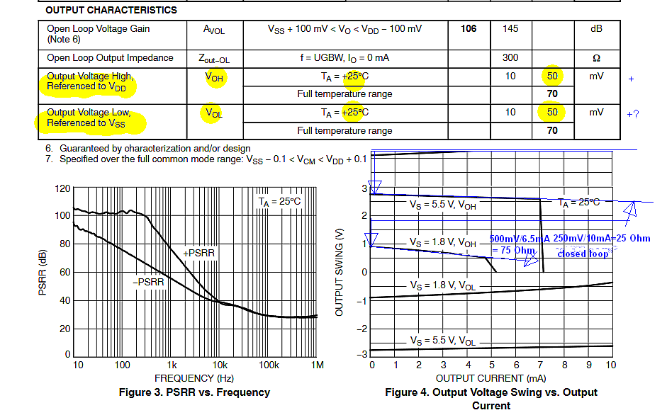
This is what concerned me about the gate drive voltage using this Op Amp as a low voltage comparator. p7 https://www.onsemi.com/pub/Collateral/NCS333-D.PDF

enter image description here

Adding a large gate resistor will help decouple reactance effects with positive feedback that you have being reduced by the output swing. The table implies a rail to rail CMOS swing output with 50mV rail offset, while the curves imply the output swing is far from Rail to Rail yet Vdd, Vss implied it is still CMOS.

After starting at it for a while, I saw the error in my interpretation now. Where the graph says Vs=5.5 meaning supply, they are using bipolar supplies here, but only define it as Vdd-Vss=Vs, so the graphs all start with a 50% swing.

Conclusion

My corrected analysis indicates you have excess gain at the resonant frequency due to 3rd order effects reducing phase margin and AC hysteresis with the load R load and C of supercap approaching the open-loop pole of the Op Amp., which may be corrected by suitable compensation.

There are 3rd order effects with RC capacitances in 3 parts (IC, FET-Ciss, Supercap) each add a pole and reducing load R pushes the pole up near the IC open-loop breakpoint.

Non-linear effects of IC: Hysteresis results in zero gain, yet the IC open loop has 130dB typ gain with a breakpoint well below 10Hz. With 10F and 1.1 Ohms, that's a bit higher.

Recommendations

The improve your stability, you can add phase-lead RC compensation or switch to a bipolar comparator or decouple the gate Ciss with a large series resistor to lower the gain at the resonant frequency with Ciss using say 10k ohm.

\$\endgroup\$
6
  • \$\begingroup\$ 1. I'm comparing to 1.24V set by TLV431B 2. Vgth of DMN1019 is quite sufficient to work from as low as ~1V according to datasheet? Gate Threshold Voltage VGS(th) 0.35 0.53 0.8 V VDS = VGS, ID = 250µA. I can't attach a picture from datasheet in comments for some reason, but even V , DRAIN-SOURCE VOLTAGE (V) Figure 1 Typical Output Characteristics graph shows that at 1V of Vgs and 1V of Vds drain current is ~2.5A? \$\endgroup\$
    – Lt_Flash
    Commented Feb 28, 2020 at 7:58
  • \$\begingroup\$ docs.rs-online.com/29e2/0900766b814b9191.pdf \$\endgroup\$
    – Lt_Flash
    Commented Feb 28, 2020 at 8:04
  • \$\begingroup\$ According to DMN1019U datasheet at Vgs 1.5V and Idrain of 2A RdsOn = ~0.012Ohm. Am I wrong? And I'm using NCS333 to compare Supercap voltage to 1.24V set by TLV431B so Op Amp powered from ~2.5V could produce a full swing, there's a voltage divider on positive input of Op Amp for that. I really appreciate your help but need some additional information how to resolve this issue. I thought I've taken into account both MOSFET Vgs(th) and RdsOn and OpAmp swing. Thanks! \$\endgroup\$
    – Lt_Flash
    Commented Feb 28, 2020 at 8:24
  • \$\begingroup\$ You did not post any measurements of Vgs or Vds. The NCS333 has typical BJT push-pull driver losses from each rail and is not Rail to Rail. \$\endgroup\$
    – D.A.S.
    Commented Feb 28, 2020 at 14:30
  • \$\begingroup\$ I hope there is no hidden load capacitance added across TLV431 Zener with only (2.5-1.24)/4.7k as per page 7 bottom \$\endgroup\$
    – D.A.S.
    Commented Feb 28, 2020 at 15:02

Your Answer

By clicking “Post Your Answer”, you agree to our terms of service and acknowledge you have read our privacy policy.

Not the answer you're looking for? Browse other questions tagged or ask your own question.