0
\$\begingroup\$

I'd like to protect my board mounted switching regulator's input from reverse polarity events without having to modify the existing run of boards we had created and populated. The primary regulator powers several of these boards that connect via pigtails down the line of cable coming off its 24V DC output.

The vast majority of examples I see online use PFETs for a high-side switch configuration, although it is sometimes noted a low-side nFET configuration works as well. I opted for the latter nFET setup just for better part availability during this supply chain madness and also to have a wider array of options for FETs with a high Vgs. The board mounted switching regulator's input allows a range of 9-36 VDC, which is one of the reasons we chose it. The max input it will ever see is right around 30V, which is the maximum output adjustability that the fine adjust potentiometer on the primary (Vreg) allows. With the load regulation specs, it could technically jump +/- 1%, so I will likely need to ensure it is dialed down to roughly 28-29V. As all of this suggests, I am trying to keep the component count to 1 nFET (with minimum Vgs = +/-30V) because I would like to install this modification as an inline solution in series with the board's input wiring.

A couple questions about this design:

1.) I chose the nFET for parts options, but also because of low Rds (anecdotally). This is also an isolated circuit and the DC negative output from our primary regulator (Vreg) does not bond to any chassis ground or common node. Is it of any concern to proceed with this design? I only ask because of the pFET's popularity in reference material, but understand why people do it.

2.) Should I anticipate any issues with the load it's powering? It's not a purely resistive load, and the regulator it's powering also powers inductive loads itself (12V solenoid valves) as depicted. I am used to installing snubber diodes for the solenoids depicted, but I am uneducated as to the risks, perhaps at a smaller scale, of what the dangers would be after disconnecting the board mounted regulator at Vin. Where does the small amount of EMF bleed in this case? Wouldn't this cause a small reverse buildup (as -Vgs) of a few volts or so? Should I be placing an additional snubber in parallel with the nFET?

3.) Assuming this hasn't been a poor approach, what form factor product can I search for that provides an easier, more modular solution for placing FETs inline on the wire, similar to a fuse assembly?

Thanks for any suggestions.

schematic

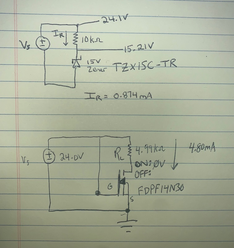
EDIT 1: Received parts, built circuit as depicted in reply, but with 15V Zener and a 10K resistor. FET used is FDPF14N30.

I was able to energize, reverse, then energize, and reverse again. After a few cycles of this, the circuit quit working. With the circuit removed, the regulator powers up again normally under normal wiring. What could have caused this? After observing the board mounted regulator kick back on and the equipment power back up normally, I did individual analysis on the components I'd used. The findings are below:

enter image description here

\$\endgroup\$

3 Answers 3

1
\$\begingroup\$

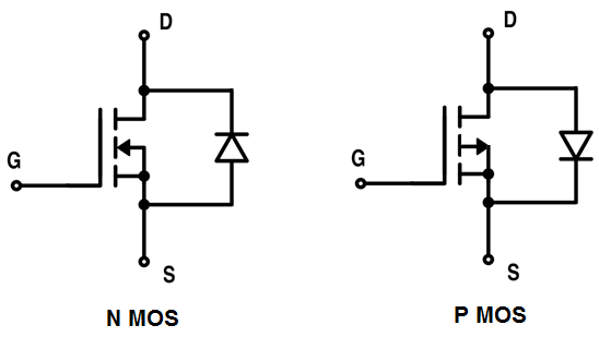
Every discrete MOSFET has an internal body-diode in parallel with the drain to source of the device. Its polarity is such that it is reverse biased in the normal usage. Many schematic symbols do show the diode but the one available here does not.

https://www.quora.com/Why-diode-is-connected-across-the-MOSFET

(Image from www.quora.com)

When using a MOSFET for reverse polarity protection as you show the diode will conduct when the power supply is reverse, this will defeat the operation of the circuit.

Luckily MOSFETs work perfectly well in the reverse direction so swapping the drain and source will achieve your objective.

I personally would also use some protection for the gate to source as you only have a few volts of margin, inductance in the wiring could easily cause a surge that would destroy the gate oxide.

Do MOSFETs have a diode built into them?

\$\endgroup\$
11
  • \$\begingroup\$ MOSFET as diode. Why just do not use diode? \$\endgroup\$
    – user263983
    Commented Feb 2, 2022 at 20:40
  • 1
    \$\begingroup\$ @user263983 - much less voltage drop and power loss \$\endgroup\$ Commented Feb 2, 2022 at 20:46
  • \$\begingroup\$ @user263983 While I can afford the voltage drop of a diode, my device's current consumption during load conditions -- upwards of 1A @ 24V -- made it seem like the heat losses (read: losses into a small, enclosed space that is often placed outdoors in heat) could be better reduced via the FET. \$\endgroup\$
    – Big Owls
    Commented Feb 2, 2022 at 20:47
  • \$\begingroup\$ According to datasheet of some MOSFETs voltage drop is same as usual silicone diode. Why not use Schottky diode if voltage drop critical? \$\endgroup\$
    – user263983
    Commented Feb 2, 2022 at 20:50
  • \$\begingroup\$ @KevinWhite I did want to touch on that in my original post but forgot to add that. This was my original intention but I goofed and got them flipped during the install, so I decided to publish the schematic of the applied version for conversation's sake. Are you saying you would expect the second regulator (onboard switching regulator) to energize? When I swap the leads to reverse polarity, it does not power on and seems to work correctly. Is this perhaps due to a limited amount of current flow in the wrong direction? \$\endgroup\$
    – Big Owls
    Commented Feb 2, 2022 at 20:53
1
\$\begingroup\$

You need to do two things: -

enter image description here

  • In red is the corrected MOSFET position
  • In purple is protection to your gate voltage due to excessive supply voltages

It's not a purely resistive load, and the regulator it's powering also powers inductive loads itself (12V solenoid valves)

Rely on the diode clampers directly on the solenoids - don't try and protect the MOSFET at a distance - protecting at the source of the problem is all you need to do.

what form factor product can I search for that provides an easier, more modular solution for placing FETs inline on the wire, similar to a fuse assembly?

It depends in the main on the current consumption of the regulator and load. Pick a MOSFET that can handle at least twice the incoming supply voltage.

Make sure that the regulator turns off on "under-voltage" before the MOSFET gets used in its linear region because it might fail. This requires careful examination of the data sheet for the regulator to ascertain what under-voltage protection it has.

what the dangers would be after disconnecting the board mounted regulator at Vin.

I'd put an extra bleed resistor of about 10k to 100k on the terminals that connect to "Vreg 24 V" (a confusing label) on the left of the diagram.

\$\endgroup\$
0
0
\$\begingroup\$

What you’re looking for is called “an ideal diode”, and there are integrated solutions that either deliver an entire such “diode”: the mosfet and the gate driver in one package, or just the ideal diode controller: the gate driver that turns an external discrete mosfet into the ideal diode you’re looking for.

You’ve not mentioned the current requirements. A couple of paralleled Schottky diodes may do well enough for your application at a fraction of the price of any equally robust ideal diode solution. Just mind the leakage current at the worst-case junction temperature in your application. No protection is ideal: you’re not removing all reverse current from the switcher input, just keeping the reverse current small enough not to damage it. This should be kept in mind.

I also don’t buy at all that the supply situation with power pmos devices is somehow much worse than nmos, at least not unless your current demands are way out there. You’re likely trying to micro-optimize Rds where in reality it won’t matter or be swamped by other effects (Rds temperature dependence, leakage currents elsewhere in the circuit, etc). If unsure: measure real performance on real circuit in real application at the temperatures of interest. Room-temp bench is not enough in your case, since micro-optimizations imply that such small differences matter for you. So you have to be consistent: if you split hairs on Rds and the “ideality” of the diode, you must have tiny margins in your design, and thus should be duly concerned about temperature and process corners.

\$\endgroup\$

Your Answer

By clicking “Post Your Answer”, you agree to our terms of service and acknowledge you have read our privacy policy.

Not the answer you're looking for? Browse other questions tagged or ask your own question.