8
\$\begingroup\$

I'm not that familiar with high-speed boards designing. Here I want to route the PCB in a part of which I've used a LAN8720A as the PHY of the ethernet system. According to what I've read about ethernet, the single-ended impedance should be 50 Ω. I've designed my Layer Stack Manager in Altium Designer as below:

enter image description here

To be honest, the results surprised me because the suggested trace width is about 120 mil, which does not seem to be normal. Did I make some mistakes in settings? Or is the 2-layer FR4 material not appropriate?


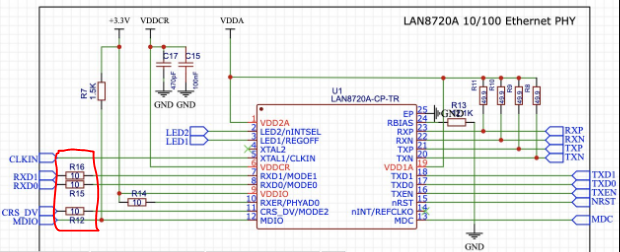
I saw this question which has the schematic below, using 10 Ω resistors for series termination.

enter image description here

Are these resistors for impedance matching ? Could I use something like that?

\$\endgroup\$
4
  • 1
    \$\begingroup\$ But your bottom layer really isn't a reference (plane) is it? From your stackup it looks like it's just another signal layer. If that's really the case then what you really have is more like a wire (or trace) in air, and your Zo is much higher than what the tool is telling you. \$\endgroup\$
    – SteveSh
    Commented Sep 12, 2022 at 15:14
  • 1
    \$\begingroup\$ As a sanity check, you can use the rule of thumb that the width of a 50Ω microstrip in FR-4 is about twice its height. (Figure 4.7, Page 144, High Speed Digital Design: A Handbook of Black Magic) \$\endgroup\$ Commented Sep 13, 2022 at 0:18
  • \$\begingroup\$ @SteveSh than you. It's a normal metallized 2layer board.. then it does matter with RMII 50MHz signals ? \$\endgroup\$ Commented Sep 13, 2022 at 4:06
  • \$\begingroup\$ @93Iq2Gg2cZtLMO thank you, I checked it and according to that the trace width should be around 3.2mm which is a very big number and cant perform it in my pcb! \$\endgroup\$ Commented Sep 13, 2022 at 4:07

4 Answers 4

5
\$\begingroup\$

No the calculation looks okay, the problem is with the two layer board the reference plane is 60 mils or more from the trace. You can think of it like this: Transmission lines need a certain width to height ratio, if the height is increased you must also increase the width.

So you either need to decrease the height, or increase the dielectric constant of the transmission line to get a smaller width. Seeing as how four layer boards are so cheap these days it might be worth just going to a four-layer board, then a non-standard stack up but you'd have to consult with your PCB manufacturer.

Another thing is it might be difficult to maintain low inductance digital pathways with the two layer board for the MII or RMII interface (especially the 50 MHz for RMII)

are these resistors for impedance matching goal? may I use something like this?

Those resistors are pull ups for the transceivers on the LAN8720A. One thing you might try if you really need a 2 layer board is keeping the traces very very short between phy and magnetics (and between magnetics and connector).

\$\endgroup\$
9
  • \$\begingroup\$ thank you @Volrage Spike for your time.. oh.. the 4layer board is not that common here yet and the prices are more than 4X of normal 2layers board. is it possible to handle this kind of project with 2layer boards? \$\endgroup\$ Commented Sep 12, 2022 at 6:49
  • \$\begingroup\$ May I use series termination resistors (about 10ohms I saw in some designs) to the job of impedance matching? \$\endgroup\$ Commented Sep 12, 2022 at 7:03
  • 1
    \$\begingroup\$ Try PCBway out of china, you will have a very hard time doing this on a 2 layer board. Again, you need to decrease the thickness of the board and or increase the dielectric. I'd give you some numbers but they'd be meaningless because you need to talk to your boardhouse and see what they can produce. The RMII needs a continuous ground plane, this will be hard or impossible to achieve on a two layer board \$\endgroup\$
    – Voltage Spike
    Commented Sep 12, 2022 at 15:18
  • 1
    \$\begingroup\$ @EricMatevosian JLCPCB does 4-layer boards very cheaply, with two choices of impedance controlled stackup (7628 and 3313 prepreg) at no extra cost. They've got full stackup info and an impedance calculator on their site. They're very popular in the hobbyist community due to their low cost and reliable quality. \$\endgroup\$
    – Polynomial
    Commented Sep 12, 2022 at 19:07
  • 1
    \$\begingroup\$ I've been not too happy with jlcpcb's soldering finish on my last batch of boards from them. \$\endgroup\$
    – Voltage Spike
    Commented Sep 12, 2022 at 21:03
4
\$\begingroup\$

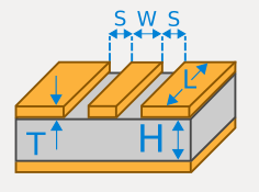
For two layer boards, a coplanar waveguide geometry usually gives more useful dimensions than a microstrip geometry. A coplanar waveguide with groundplane distance H = 1.5 mm, trace width W = 0.4 mm, trace spacing S = 0.1 mm gives roughly 50 ohms impedance. For differential pairs, a coupled microstrip line can work also.

Coplanar waveguide image, screenshot from KiCad

But also consider the speed of the signals you are routing and the length of the traces. The 10 ohm series resistors slow down the rise and fall time of the signal, reducing the effect of any impedance mismatches. A common rule of thumb is that impedance matching is not needed if the trace length is less than quarter of the electrical length of the rise time.

It is often hard to find exact specifications for the rise and fall times of digital signals, as it depends on the capacitive load and output impedance of the pin. With the 20 ns period of the RMII interface clock, the rise times could be several nanoseconds without disturbing the bus function. This in turn would give a limit of about 10 cm before needing impedance matching. The series resistors provide an easy way to adjust the rise time based on measuring a prototype.

\$\endgroup\$
2
  • \$\begingroup\$ thank you @jpa for your reply! some good news here! my traces length are below 5cm. and they are well length matched with tolerance +/-20mil. (Tx lines with Tx line and Rx line with Rx line - this is about both signals lines between PHY & MAC __ and__ PHY & magnetics) so what do you suggest with this situation? should I use termination resistors in all of signals ? \$\endgroup\$ Commented Sep 13, 2022 at 4:25
  • 1
    \$\begingroup\$ @EricMatevosian Putting series resistors at the driving end of each high-speed signal would reduce EMC emissions and make it easy to try out different values if you hit any problems. But in practice it is very likely to work without the resistors also. \$\endgroup\$
    – jpa
    Commented Sep 13, 2022 at 6:03
3
\$\begingroup\$

That is an expected result. Not the numbers but as a concept of using standard 1.6 millimeter thick board for this.

It is too thick to have sensible 100 ohm differential traces over a ground plane.

\$\endgroup\$
3
  • 1
    \$\begingroup\$ Is OP's bottom layer really a GND plane? In the stackup it looks like it's signal. \$\endgroup\$
    – SteveSh
    Commented Sep 12, 2022 at 15:16
  • \$\begingroup\$ thank you @Justme for your reply \$\endgroup\$ Commented Sep 13, 2022 at 4:31
  • \$\begingroup\$ @Justme - the answer is useful but I suggest that "fleshing it out" somewhat would be a good idea. \$\endgroup\$
    – Russell McMahon
    Commented Sep 14, 2022 at 3:09
2
\$\begingroup\$

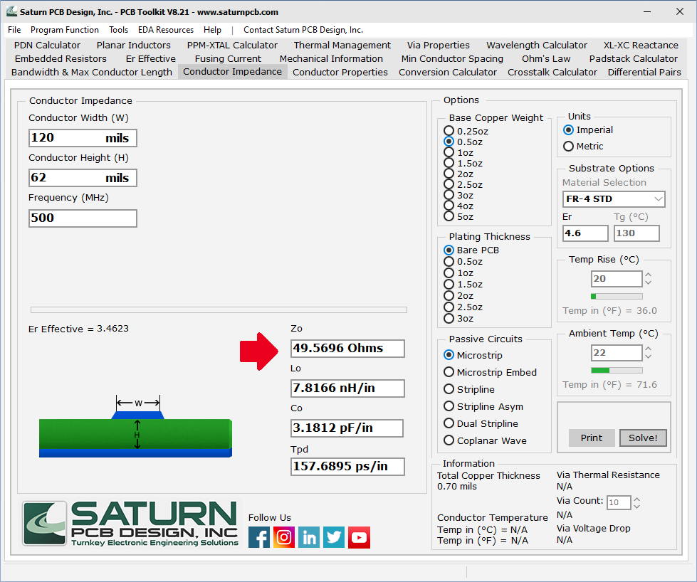
As others have mentioned, for a 50 Ohm microstrip, 62 thou above a plane, a 120 thou trace for FR4 is about right. As a second opinion, here is what Saturn PCB toolkit says:

Screenshot from Saturn PCB toolkit

If a 120 thou trace is too wide, moving the plane closer to the trace will help. This can be done by using a thinner board, or going to four layers (signal / plane / plane signal).

\$\endgroup\$
1
  • \$\begingroup\$ thank you for your reply , unfortunately choosing a thinner board like 1mm or even 0.8 do not provide a appropriate trace width for my PCB \$\endgroup\$ Commented Sep 13, 2022 at 4:27

Your Answer

By clicking “Post Your Answer”, you agree to our terms of service and acknowledge you have read our privacy policy.

Not the answer you're looking for? Browse other questions tagged or ask your own question.