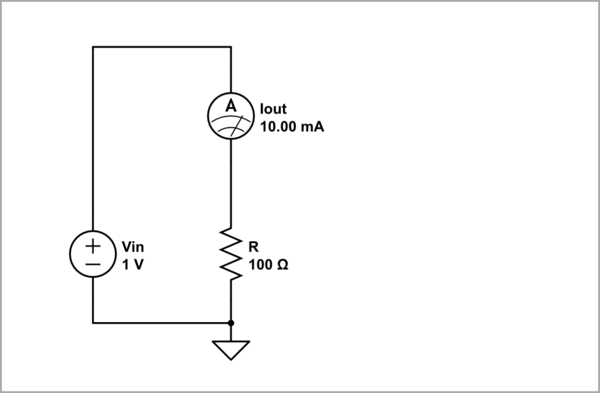
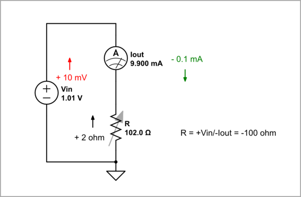
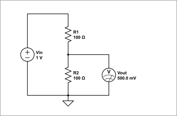
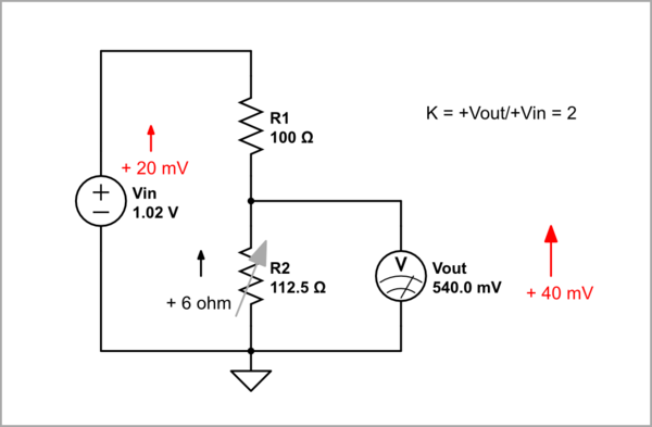
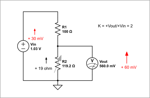
Don't confuse a DC input potential, denoted with capital \$V\$, and small signal AC fluctuations, denoted by a small \$v\$. In addition, you should be aware that in this context (which is very common), small \$v\$ generally refers to the amplitude of the tiny fluctuations, not to its potential at any particular time.
That formula in the book is referring to small signals, small AC variations on top of (superimposed onto) a steady DC potential. So, if you image that you have an average DC potential across the diode of 0.1V, to bias the diode, that might be written \$V_{BIAS}=0.1V\$, and superimposed onto that you have a very small (in comparison to \$V\$) sinusoidal voltage, a "signal" \$v_{SIG}\$ of amplitude 10mV. The expression describing the combined signal \$V\$, as it varies over time, might be written:
$$ V = V_{BIAS} + v_{SIG}sin(\omega t) $$
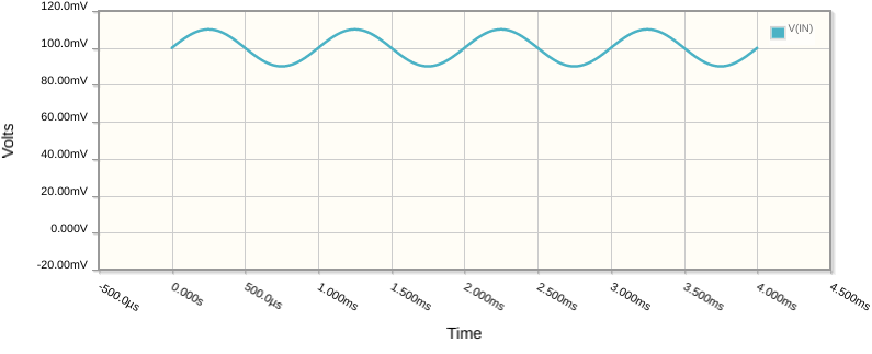
In the following graph of V against time, you can see the DC offset \$V_{BIAS}=+0.1V\$ as its average value above the x-axis, and \$v_{SIG}=0.01V\$ is the amplitude of the small sinusoidal fluctuations above and below that average:

In that example \$v_{SIG}=0.01V\$ may not be considered "small", but I had to make it significant enough to see the principle at work in the graph. In the context of this question "small" means much smaller than this, and in the context of simulation and "small signal AC analysis" it means infinitesimally small.
To reiterate the most important point, small \$v\$ refers to the amplitude of the AC component of the waveform, not to any absolute value at any particular instant in time.
You may have already figured out where this is going, but I'll continue.
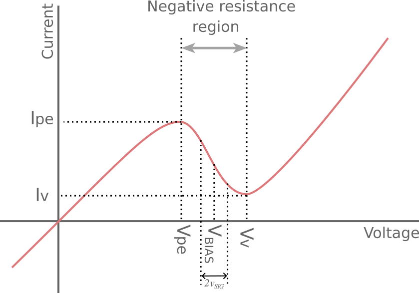
Let's take a look at a tunnel diode's VI curve, which I borrowed from www.electronics-notes.com, and then annotated a bit:

The region of interest is between \$V_{pe}\$ and \$V_V\$, which are actual potentials, not amplitudes. In this region, as voltage rises current falls, and the diode behaves as if it had negative resistance. That resistance will be calculated as the run-over-rise slope in that region, and we will bias the diode at some point near the middle of that region, at \$V_{BIAS}\$.
As long as the voltage \$V\$ across the diode does not deviate far from \$V_{BIAS}\$, meaning that whatever signal we superimpose onto \$V_{BIAS}\$ does not cause us to leave that region (in other words, its amplitude \$v_{SIG}\$ is small, compared to \$V_V-V_{pe}\$), then the diode will behave as if it were a negative resistance.
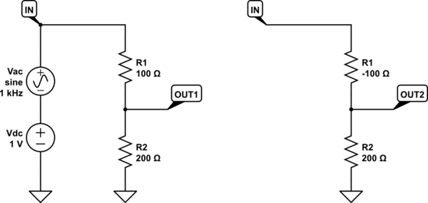
Below left is a simple resistive potential divider, with two positive resistances, and on the right I've replaced R1 with a negative resistance.

simulate this circuit – Schematic created using CircuitLab
Obviously the left-hand "normal" circuit has the the following relationship between \$V_{IN}\$ and \$V_{OUT1}\$:
$$ V_{OUT1} = V_{IN}\frac{R_2}{R_2+R_1} $$
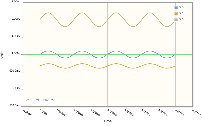
You might be surprised to learn that the right hand circuit, with that negative resistance, has the exact same relationship between \$V_{IN}\$ and \$V_{OUT2}\$. Here are those relationships plotted, with \$V_{IN}\$ blue, \$V_{OUT1}\$ in orange, and \$V_{OUT2}\$ in tan:

The important take away here has nothing to do with the instantaneous values of any waveform, it's all about the relative amplitudes of them. That negative resistance is clearly causing the circuit to produce an output with greater amplitude than the input.
Obviously you couldn't build this second circuit with any real-life resistors, since negative resistors don't exist. You could build an active module using op-amps, to emulate a negative resistance, though, and you'd see this same result.
In the relationship
$$ V_{OUT2} = V_{IN}\frac{R_2}{R_2+R_1} $$
if the denominator is larger than the numerator here (as is the case when both resistances are positive), this represents attenuation. If R1 is negative, though, the denominator can be smaller, causing amplification. In the graph you can clearly see that the amplitude of the sinusoidal part of \$V_{OUT2}\$ is greater than that of \$V_{IN}\$.
We are relating instantaneous values of \$V_{OUT2}\$ with a corresponding (in time) instantaneous value of \$V_{IN}\$, and you can see proportionality between \$V_{OUT2}\$ and \$V_{IN}\$. That is, if \$V_{IN}\$ doubles, then so does \$V_{OUT2}\$. In other words, the gain \$\frac{R_2}{R_2+R_1}\$ is constant.
Therefore we can also say that a change in \$V_{IN}\$ will also result in a proportional change in \$V_{OUT2}\$, by the same factor. Let's rewrite the input as a combination (sum) of some DC offset potential \$V_{IN(DC)}\$ and a small sinusoidal component \$V_{IN(AC)}\$, assuming that the DC part remains constant:
$$ V_{IN} = V_{IN(DC)} + V_{IN(AC)} $$
Do the same for output \$V_{OUT2}\$:
$$ V_{OUT2} = V_{OUT2(DC)} + V_{OUT2(AC)} $$
Now we can plug these into the relationship above:
$$
V_{OUT2(DC)} + V_{OUT2(AC)} = (V_{IN(DC)} + V_{IN(AC)})\frac{R_2}{R_2+R_1}
$$
Expand and rearrange to leave only \$V_{OUT2(AC)}\$ on the left:
$$
V_{OUT2(AC)} = V_{IN(AC)}\frac{R_2}{R_2+R_1} + \overbrace{V_{IN(DC)}\frac{R_2}{R_2+R_1} - V_{OUT2(DC)}}^\text{Constant DC offsets}
$$
Notice that, as long as we keep all DC components constant, the last two terms on the right are constant values, and can be replaced by an arbitrary, unchanging value \$V_{OFS}\$. In practice this constant accounts for diode biasing and whatever other DC offset potentials are present:
$$
V_{OUT2(AC)} = V_{IN(AC)}\frac{R_2}{R_2+R_1} + V_{OFS}
$$
Now \$V_{IN(AC)}\$ and \$V_{OUT2(AC)}\$ are the "signals" of interest, the small fluctuations in input and output potential, and according to this last equation, output fluctuations are a factor of \$\frac{R_2}{R_2+R_1}\$ different from the input.
To paraphrase that, input and output amplitudes are related by that factor. We may write:
$$ v_{OUT2} = v_{IN}\frac{R_2}{R_2+R_1} $$
where \$v_{IN}\$ and \$v_{OUT2}\$ are amplitudes. Otherwise put, we are simply saying that the amplitudes of the AC components are also proportional, and the constant of proportionality is the gain of the potential divider \$\frac{R_2}{R_2+R_1}\$. However, in doing so, we can no longer infer anything about the actual instantaneous potentials, or DC offsets, only their relative amplitudes.
Anyway, since R2 is to be replaced by a tunnel diode, what you now have is a an element that exhibits a negative resistance. We have been very careful to choose all DC offset potentials and potential differences in the circuit to ensure that the diode is squarely "positioned" (biased) in that region of negative resistance, where an increase of voltage across it will result in a decrease of current through it.
We then make the assertion that we won't apply (superimpose) any potential change large enough to exit that region, that all potential changes will be "small", which is another way of saying our AC signals will have small amplitude, and the DC potentials will remain steady. If we replace \$R_1\$ with \$r_t\$, the diode's effective "small signal AC" resistance in that region, the following relationship remains true:
$$ v_{OUT2} = v_{IN}\frac{R_2}{R_2+r_t} $$
Since \$r_t\$ is negative, the denominator is smaller, and there is amplification.

