12
\$\begingroup\$

I have an NMOS that is switching too fast for my application. Into the gate I am sending a logic-level square wave (PWM). Unfortunately for me, as expected, the output is also a near square wave.

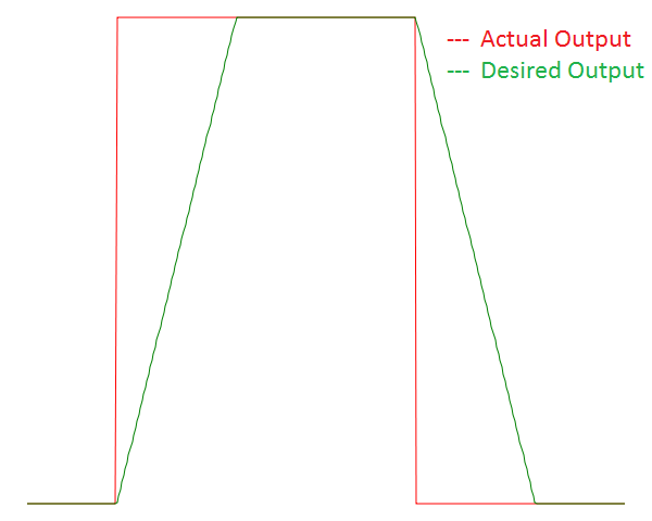
How can I get the Vout to be more trapezoidal? Or said another way, what is the simplest modification I can make to decrease the slew rate at the output?

Note: (Vin) is the voltage applied at the gate of the NMOS & (Vout) is the voltage seen at the drain of the NMOS.

enter image description here enter image description here

\$\endgroup\$
3
  • \$\begingroup\$ Just a note, since everyone is wondering. The resistor represents a 50 watt load, that will be pulsed for only 0.5sec. However, I can't turn it on too fast. \$\endgroup\$
    – hassan789
    Commented Mar 20, 2014 at 17:02
  • \$\begingroup\$ Given the updated info, I have removed my answer \$\endgroup\$
    – Adam Head
    Commented Mar 20, 2014 at 17:10
  • 2
    \$\begingroup\$ If you're diving a 50 W load, a slower turn-on may result in significant power dissipation in the MOSFET. If you can PWM the ramp, that would make it easier. \$\endgroup\$
    – Nick T
    Commented Mar 21, 2014 at 4:31

4 Answers 4

15
\$\begingroup\$

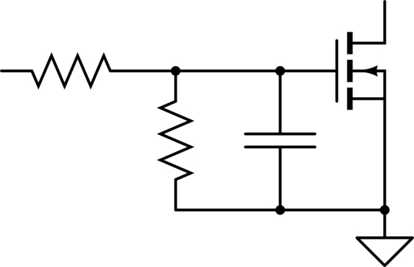
The only control you have over the resistance of the FET is the gate-source voltage. You need to slow down the change of that voltage. The most common way of doing that is an RC filter at the gate. Put a resistor between your drive source and the device gate, and the gate's parasitic capacitance will form an RC filter. The bigger the resistor, the slower the turn-on and turn-off.

If the resistor gets too big, you can have noise immunity issues (false gate triggers and such), so past a certain resistor value (maybe in the 10k-100k range) you're better off adding capacitance gate-source to slow the switching down further.

As a general rule, I always put an RC filter with a pulldown resistor on all FETs. This allows control of the rise-time, and provides improved noise immunity.

schematic

simulate this circuit – Schematic created using CircuitLab

Keep in mind that any time your FET spends not fully "on" or "off", it sees increased losses. If it's on, the device has very low voltage across it. If it's off, the device has no current through it. Either way, low loss. But if you're in between, the device sees both voltage and current, meaning its power dissipation is far greater during that period. The slower you switch, the greater that loss becomes. At what point it becomes a problem depends on the FET, the source, and the switching frequency.

\$\endgroup\$
1
14
\$\begingroup\$

Not enough Miller time? Just extend it.

Spehro has the right approach here. I am going to ride his coat tails and expand on the idea a little, because it is such a good idea for this kind of thing.

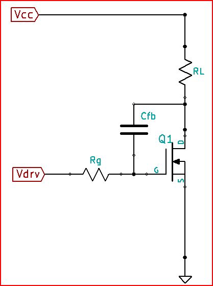
\$C_{\text{dg}}\$ is special in a FET because it provides negative feedback to the gate. Part of what that means is that it also gets multiplied by the transconductance (\$g_{\text{fs}}\$) of the FET. So, it has a larger effect than it's size would lead you to believe. But, let's forget about \$C_{\text{dg}}\$ for now and instead add an external capacitor from drain to gate (\$C_{\text{fb}}\$), because if you really want to slow down the rise and fall times of the FET that's what you'll do. Here is a schematic to help illustrate:
enter image description here

As \$V_{\text{drv}}\$ rises and \$V_{\text{ds}}\$ falls you can probably see how \$R_g\$, \$R_L\$, \$g_{\text{fs}}\$, and \$C_{\text{fb}}\$ all play a part in limiting the value of \$V_{\text{gs}}\$. Small signal transfer function of \$V_{\text{ds}}\$ relative to \$V_{\text{drv}}\$ is:

\$-\frac{R_L}{s C_{\text{fb}} \left(g_{\text{fs}} R_g R_L+R_g+R_L\right)+1}\$

And, \$R_g\$, \$R_L\$, \$g_{\text{fs}}\$, and \$C_{\text{fb}}\$ are all involved in forming the pole. (Note, all the FET capacitances are left out here for clarity.)

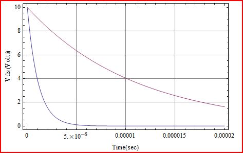
To show approximately how this works out, put in some values into a very simplified model. \$R_g\$ = 1000 Ohms, \$R_L\$ = 2 Ohms, \$V_{\text{drv-pk}}\$ = 5V, \$V_{\text{cc}}\$ = 10V, \$g_{\text{fs}}\$ = 5 S.

Here is a plot of \$V_{\text{ds}}\$ on application of \$V_{\text{drv-pk}}\$.
enter image description here

The blue curve is \$C_{\text{fb}}\$ = 100pF, and the purple curve is \$C_{\text{fb}}\$ = 1000pF. Of course, switching loss will be huge and huger. It should also be mentioned that adding a Miller feedback capacitor like this will make the circuit more sensitive to dV/dt turn on.

\$\endgroup\$
3
  • \$\begingroup\$ but if I introduce a dV/dt (pretty much a voltage spike) at Vgs, it will turn on only momentarily right? \$\endgroup\$
    – hassan789
    Commented Mar 21, 2014 at 13:28
  • \$\begingroup\$ @hassan789 Well, dV/dt events are momentary one way or the other. It's charge injection from the drain to the gate through Cfb, and depends on Vcc and the true nature of the load. If Vcc appears quickly and the load has a capacitive element dV/dt might be enough to cause some conduction. A rough estimate could be made of tolerable dV/dt with dV/dt~Vth/(RgCfb). Or dV/dt might extend turn off beyond expected. Just need to be aware. \$\endgroup\$
    – user16497
    Commented Mar 21, 2014 at 16:18
  • \$\begingroup\$ "But, let's forget about Cdg for now and instead add an external capacitor from drain to gate (Cfb)" Do you mean "Let's forget about internal Cdg and add an external Cdg"? \$\endgroup\$
    – endolith
    Commented May 2, 2023 at 17:06
8
\$\begingroup\$

You can add a series resistor to the gate. That's often done to slow rise-fall times in order to reduce EMI or prevent excessive overshoot. Obviously this increases switching losses (but not conduction losses), so there is a trade-off. As well as causing the switching to slow, it will also add a delay time, so keep that in mind if there is a chance of cross-conduction or similar problems.

The slope you get for a given value of gate resistor will depend on the capacitances from gate to source and gate to drain, as well as the value of Vcc. While the MOSFET is switching, the resistor supplies the current to charge \$C_{GS}\$ as well as the current to charge \$C_{DG}\$ between Vcc and 0. The total amount of charge is often specified in the datasheet (under given conditions) as the gate charge (measured in nanocoulombs). Because of the Miller capacitance (\$C_{DG}\$) the nature of the load comes into play as well.

\$\endgroup\$
3
  • \$\begingroup\$ Do I run the risk of not fully turning on the FET by doing this? \$\endgroup\$
    – hassan789
    Commented Mar 20, 2014 at 17:05
  • 1
    \$\begingroup\$ @hassan789: Assuming the square wave doesn't flip before it has saturated, no. \$\endgroup\$ Commented Mar 20, 2014 at 17:14
  • \$\begingroup\$ @hassan789 No, as I said it won't increase conduction losses. The gate voltage after some time will be essentially the same as without the resistor, since the gate leakage should be very small. Of course the MOSFET won't be fully turned on during the switching (increasing the power dissipation), but I think that's what you asked for. \$\endgroup\$ Commented Mar 20, 2014 at 17:14
3
\$\begingroup\$

What are the operating condition of your MOSFET?

When used as a switch, the MOSFET is most of the time in two states:

  • Blocked: High \$V_{\text{ds}}\$ voltage, no current -> no dissipated power
  • Conduction: Very low \$V_{\text{ds}}\$ voltage (\$I_{\text{d}} \times R_{\text{ds_on}}\$), high current (\$I_{\text{d}}\$) -> small dissipated power (\$R_{\text{ds_on}} \times I_{\text{d}}^2\$)

The MOSFET is in a third state, during a very small amount of time. And this third state is when it is conducting a little: - Non negligible \$V_{\text{ds}}\$ voltage, non negligible current. \$I_{\text{d}} \times V_{\text{ds}}\$ may be high! -> possibly big dissipated power.

If you plan, by design, to put your MOSFET longer into this third state, you have to ensure that the increase of the temperature of its junction won't let it pass above the maximum allowed temperature for that junction. (found in the datasheet) Reducing the slew rate of a MOSFET has to be carefully studied.

I don't know what you are driving with it. If it is a LED and you want to have it becoming brighter and brighter, but slowly, you would better use a PWM on the gate of your MOSFET and still use it as a switch. If the PWM is very fast, it won't be noticeable to a human eye.

The same approach is also valid for driving a motor.

\$\endgroup\$
1
  • \$\begingroup\$ Actually, im trying to exploit the 3rd state... for my application, I want the FET to remain in the 3rd state longer (I know this means that the fet will burn up). But it will only be in the linear state for a small amount of time \$\endgroup\$
    – hassan789
    Commented Mar 20, 2014 at 16:59

Your Answer

By clicking “Post Your Answer”, you agree to our terms of service and acknowledge you have read our privacy policy.

Not the answer you're looking for? Browse other questions tagged or ask your own question.