1
\$\begingroup\$

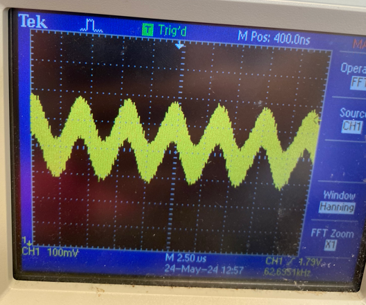
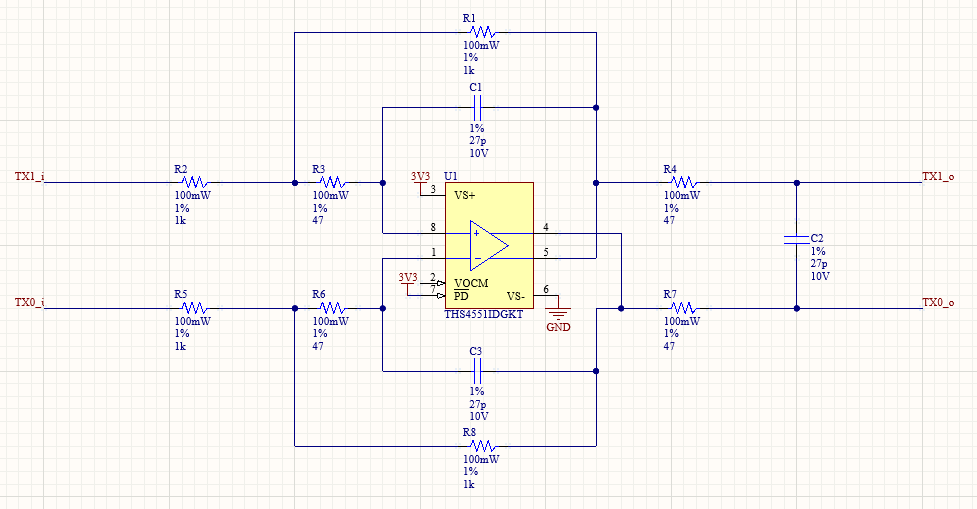
I designed this circuit. It is a fully differential amplifier of gain one. I am getting this ringing and noise on the output of tx1_o

Blue is where the probe is and ground is on circuit's ground.

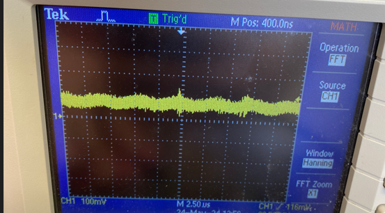
Here is with the probe on 1x enter image description here

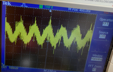
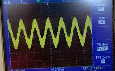
I have put a 100nF cap in series with the measurement point to AC couple the signal into the RFSoC ADC. This is on the leg of the cap that is AC coupled and on the ADC side. (10x probe)

enter image description here

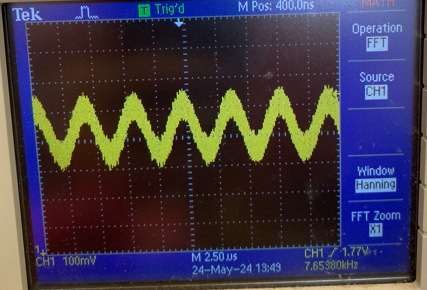
This is measuring on the leg of the cap that has the source signal, the opposite leg of the one depicted above. Still too noisy but spikes are gone on this side. Note: this is the same place of measurement depicted in the 1x probe picture (below is 10x probe).

enter image description here

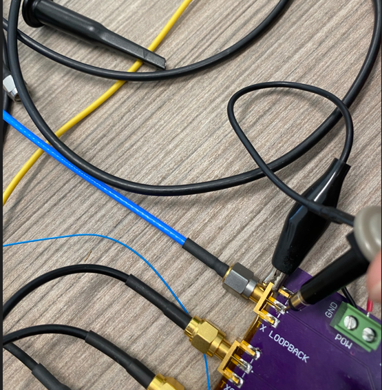
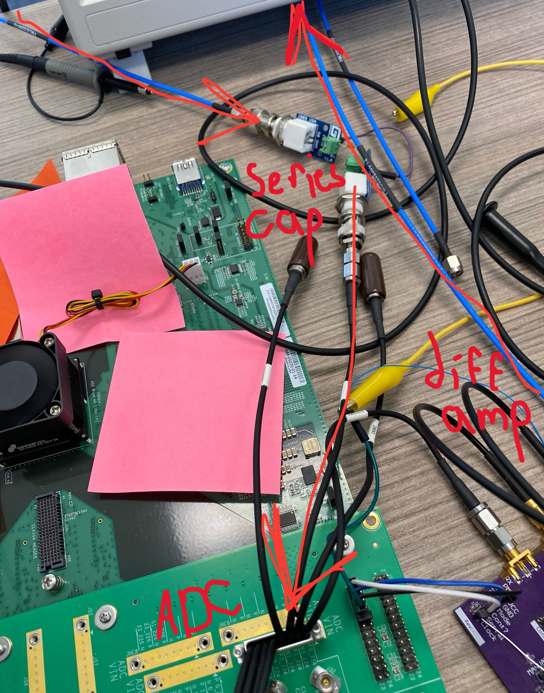
Here is where I am taking a measurement (this is on the signal generator side):

enter image description here

Path that the signal is taking:

enter image description here

Here is the signal measured at the source tx_loopback or tx0 WITHOUT the ADC connected:

enter image description here

Here is the signal measured at the source tx_loopback or tx0 WITH the ADC connected (it is more attenuated and noisy):

enter image description here

What can I do to remove this ringing and what could be causing it?

enter image description here

\$\endgroup\$
10
  • 1
    \$\begingroup\$ Could you use a 10x probe, show us the input signal, and show us where the probe tip and probe ground are, please? What are the differences between a x1 and a x10 osciloscope probe \$\endgroup\$ Commented May 24 at 17:30
  • \$\begingroup\$ @AndrewMorton Thanks for your reply. I have edited the above post and included more information to help. \$\endgroup\$
    – Ishmael
    Commented May 24 at 17:58
  • 1
    \$\begingroup\$ @Ishmael do you have any capacitance on your power rails? Also, a clearer schematic would be helpful (its impossible to read most of the text) \$\endgroup\$
    – BeB00
    Commented May 24 at 18:15
  • \$\begingroup\$ @BeB00 Hey thanks for responding. I have included a better picture of the schematic as well as some more pictures for clarity. \$\endgroup\$
    – Ishmael
    Commented May 24 at 18:49
  • \$\begingroup\$ you have long wires all over the place - does anything change when you move the wires around? \$\endgroup\$
    – BeB00
    Commented May 24 at 19:49

1 Answer 1

1
\$\begingroup\$

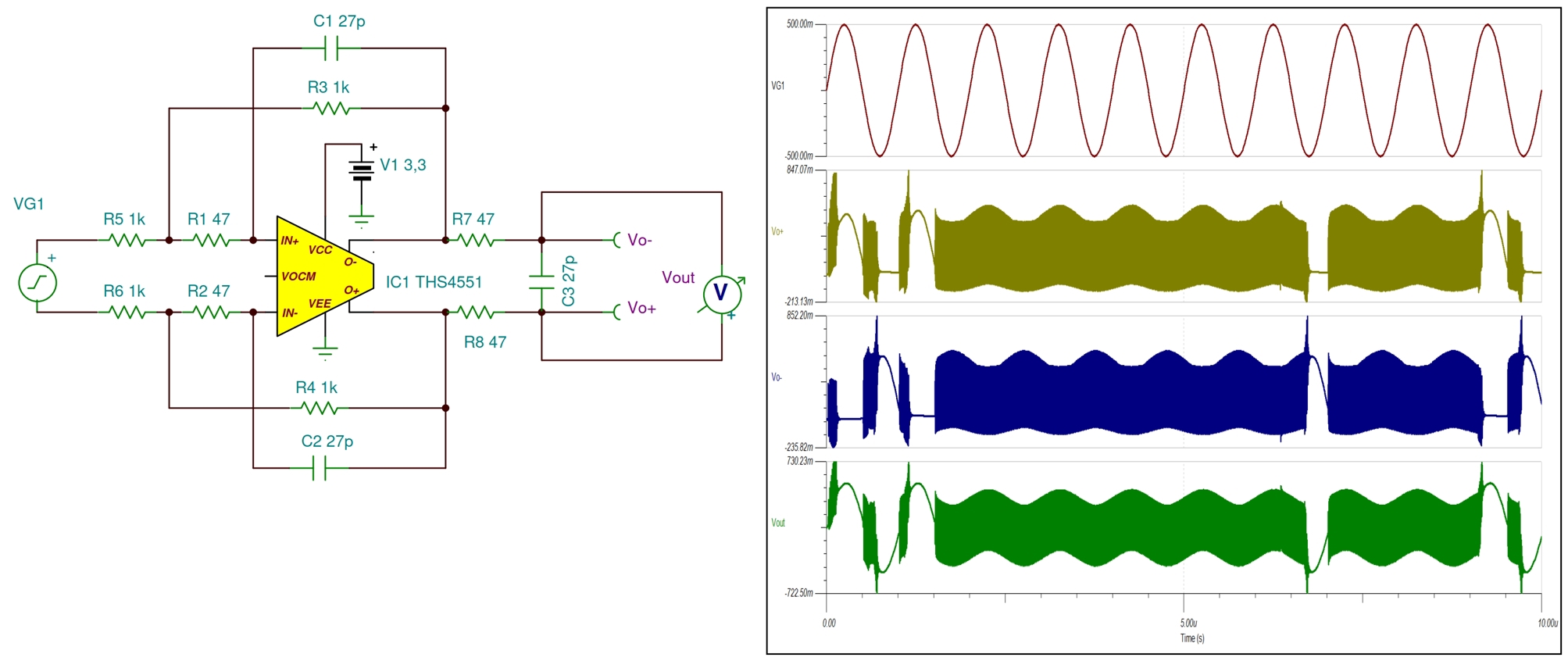
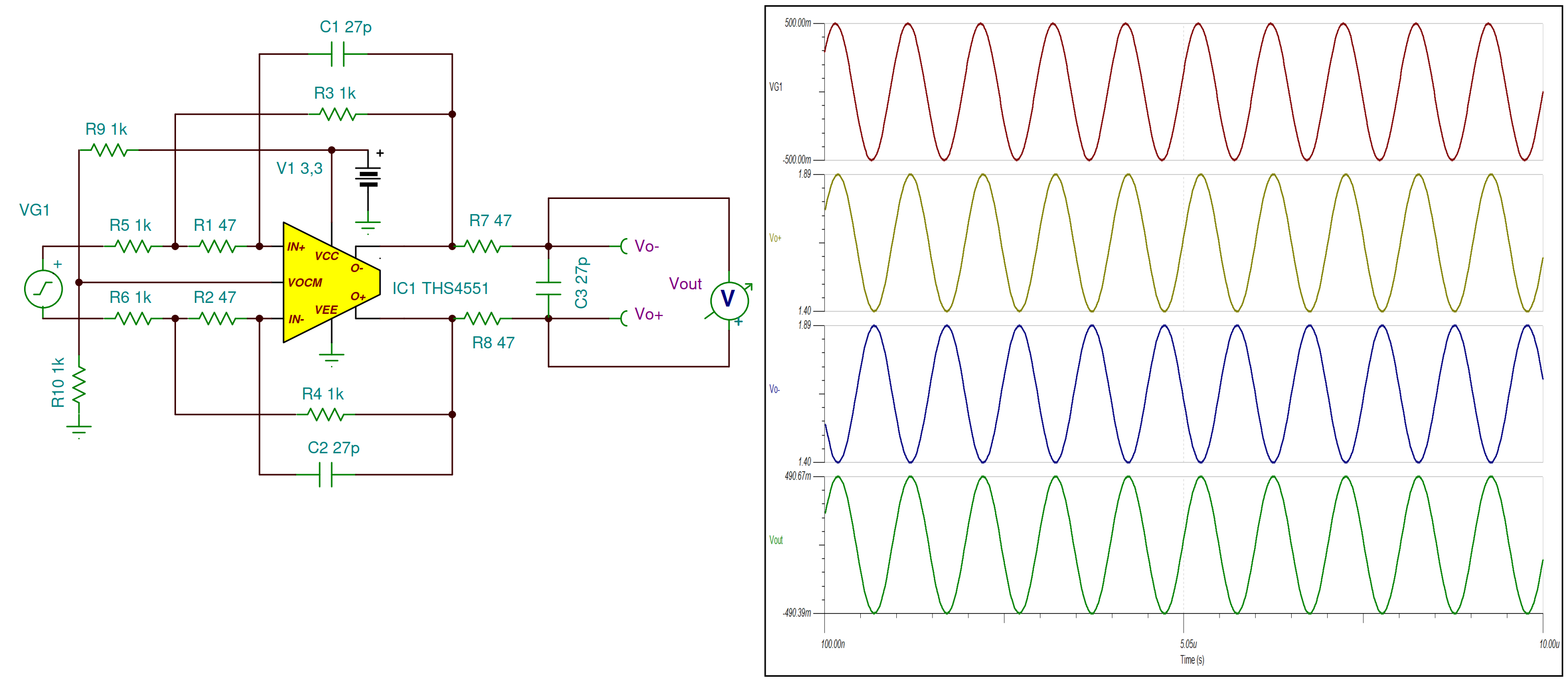
It's rare that simulation can help in such cases, but it might now. The original schematic shows a high frequency oscillation when the supply voltage is applied. enter image description here The amplitude of this can be reduced by lowering the value of the resistors and capacitors, but it is not completely eliminated. If the input signal is a square wave, it occurs only at the edges, for a sine wave, it is more pronounced the smaller the input signal. The impedance of the VOCM input is quite high (Ib=11 µA), capacitive filtering improved it a bit, but did not solve the original problem. The only option was to produce a half supply voltage with a lower impedance. This clearly fixed the circuit in the simulation with the original components without any other modifications. Based on this suggestion plus two 1 kΩ resistors and we will see if the simulation was useful (R9 and R10). enter image description here

\$\endgroup\$

Your Answer

By clicking “Post Your Answer”, you agree to our terms of service and acknowledge you have read our privacy policy.

Not the answer you're looking for? Browse other questions tagged or ask your own question.