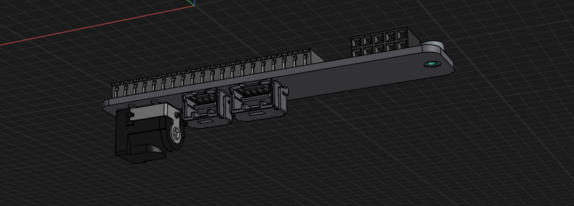
I have this rough layout for a design with some serious space constraints:
It has connectors on both sides and the layout rules out through-hole soldering. I only have access to a Hakko IR preheater for SMD soldering, which will require low-temp paste for both sides. I'm worried about the bottom-side components falling off as the contact pads are very small and I doubt I can rely on surface tension to hold things in place. Suitable glue is very hard to find.
I was thinking about splitting up the design into two parallel boards flat against each other. Something like this:
I could join the boards with a few plated throughholes, pieces of solid core wire, and solder on both sides. I only need to get four traces across so this seems easy - but then again, I am out of my depth here.
Any easy advice for doing this with one board? I looked at glue datasheets and availability all morning, and nothing feasible came up.
If I was to use two boards, any caveats someone new to the field might miss? Would reasonable mechanical strength be achieved by using, say, 6 PTH joints? Should I leave the bottom sides of both boards (the ones facing each other) blank, or could I use them as a common ground plane if electrically joined with multiple connections?
In case it matters, I'll have some smaller components (flyback diodes, a fuse, a couple of ceramic capacitors) on the boards; these are not shown on the CAD design.


