0
\$\begingroup\$

The following circuit shows a CD4060 in a timer circuit, intended to hold a relay (with a transistor driver) on for about an hour, then turn it off. I want to have a reset switch so that at any time, I can push it to start the timing from an hour again.
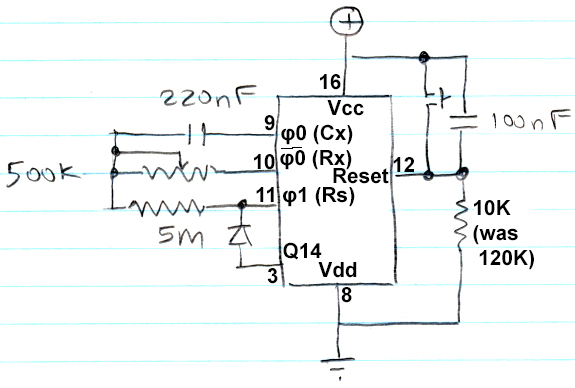
The circuit is shown in simplified form. It shows mostly the power and inputs. For testing, the outputs are connected to a bank of LEDs with current-limiting resistors, showing every available state (Q4-Q10, Q12-14), but I did not show that in the diagram, for simplicity. It counts correctly. The relay is not in the circuit yet.

ONE output is shown, Q14 at pin 3, with a diode whose purpose is to latch the timer, to stop counting when it reaches Q14, or about one hour. The latching effect works correctly. Q14 is also connected to an LED as described above.

The 120K resistor and the 100nF capacitor are a power-on reset circuit, and that has been working every time I tried. "Trying" means turning of the master power switch (before the power transformer in the power supply) and then turning it on again.

PROBLEM: the only thing that does not work correctly is the manual reset pushbutton across the 100nF capacitor. As I understand it, the 4060 RESET (pin 12) can be connected HI to achieve a reset. However, pushing the button, whether quickly or for a second or two, usually results in a non-zero state for the 4060 registers, typically with Q5-Q9 HI.

Why does the manual reset not clear all registers to zero, and how do I fix it?

UPDATE: in the original post, the resistor from pins 12 to 8 was said to be 1M, but it was 120K. Per suggestions in comments and answer, I changed it to 10K. Reset button works as long as I don't hold it down longer than say 1/2 second. When holding it down, releasing it leaves the registers in a non-zero state.

\$\endgroup\$
17
  • 1
    \$\begingroup\$ Please can you put pin numbers outside the IC 'box' and the signal names inside, alongside each connection. Otherwise people would have to find a datasheet to understand the schematic and they won't, I'm afraid. Thanks. \$\endgroup\$
    – TonyM
    Commented Jun 6, 2017 at 16:09
  • \$\begingroup\$ Data sheet link added @TonyM \$\endgroup\$
    – Trevor_G
    Commented Jun 6, 2017 at 16:10
  • 1
    \$\begingroup\$ 1M seems a tad high for a pulldown... \$\endgroup\$
    – Trevor_G
    Commented Jun 6, 2017 at 16:15
  • 1
    \$\begingroup\$ Two words: contact bounce. \$\endgroup\$
    – JRE
    Commented Jun 6, 2017 at 16:23
  • 1
    \$\begingroup\$ @Trevor, yes, a monostable in this mode is inherently a debounce circuit. Thanks for putting the datasheet link in. A formatted schematic's best though, attracts a wider audience and hopefully better answers :-) I dunno if what you're calling noise effects are what I'd call pin leakage current effects, with the huge resistors but if so, spot on. \$\endgroup\$
    – TonyM
    Commented Jun 6, 2017 at 16:49

4 Answers 4

1
\$\begingroup\$

In general I think your resistor values are far too large.

The leakage current on the reset pin will leave quite a bit of voltage across the 1M resistor which can be an issue. Similarly, the oscillator components are high values which leaves you open to noise in that circuit.

\$\endgroup\$
4
  • \$\begingroup\$ I assumed the large 1M resistor was a matter of having a long enough power-on reset pulse. I think the time is the usual RC product, right? Can the capacitor be electrolytic for power-on reset? What value would you use for resistor, capacitor for the power-on reset circuit? \$\endgroup\$
    – Mark Colan
    Commented Jun 6, 2017 at 20:45
  • \$\begingroup\$ The value I used for the timing resistor is a 500k trimpot, which would be set close to 500k. I surveyed similar circuits (at least one was obviously wrong! and the author did not correct it even when someone pointed it out in a comment). They tended to use 500k and even 1M and higher timing resistances. Unfortunately the datasheet did not offer much guidance for the RX and CX values, other than giving the formula as 2.2*RX*CX for the period of the oscillation. \$\endgroup\$
    – Mark Colan
    Commented Jun 6, 2017 at 20:51
  • \$\begingroup\$ See the update in comments above. \$\endgroup\$
    – Mark Colan
    Commented Jun 6, 2017 at 21:02
  • \$\begingroup\$ @MarkColan yes the spec sheets are woefully under documented in that arena which is weird for a timer chip. General rule of thumb is, if you are not running off a battery and need to REALLY minimize drain, lower values are less susceptible to noise. EIther way I'd drop the reset resistor at least a factor of 10. Current draw is not an issue with that one. \$\endgroup\$
    – Trevor_G
    Commented Jun 6, 2017 at 21:05
1
\$\begingroup\$

You don't show a bypass capacitor across the power supply. Be sure you have at least 100nF, preferably 1uF ceramic near the chip. And make sure you are not doing anything to disrupt it- if you are having problems now, you will have worse problems when a relay and noisy contact switching enters the scenario.

Just to be clear -the only way to get the sort of effect you describe is by an improper power rail transient.

I don't think your values are a problem, but I would definitely get rid of that RC reset circuit and replace it with something more reliable. If your supply rail is 5V, 3.3V etc. there are plenty of commercial chips that are infinitely better than an RC circuit.

\$\endgroup\$
1
\$\begingroup\$

Just out of the box, can you use a cheap microcontroller here?? Because that way, you can have accurate and adjustable time delay from microseconds to years. And you can build any sort of reset/update logic for your timer.

The cheapest STM8 controllers come for less than a dollar.

The RC delay schemes like this one used with 4060 are not much accurate or reproducible for times more than a few seconds.

\$\endgroup\$
1
  • \$\begingroup\$ Indeed, the approach being taken in the question is an unwise one for solving a real problem. \$\endgroup\$ Commented Dec 22, 2018 at 21:17
-1
\$\begingroup\$

It's probably VSS (pin 8 labeled Vdd in the diagram) not connected to ground.

The resistor values are obviously sufficient else it would not work at all. however the datasheet calls for RS to be between 2 and 5 times RX so 1M might be a better choice there. (figure 12)

And VDD must be connected because there's no other connection to the positive supply.

The diode is working beacuse it stops and the end of count

That only leaves the VSS connection. with that connection broken the current exits through the reset pin's protection diodes and the 10K resistor. feeble at that current must be a 4060 does not need a lot of current, and is not fussy about the supply voltage and the timing parts are a much higher resistance. But pressing the reset button would now cut the only power supply the chip has - resulting in an incomplete reset.

\$\endgroup\$
2
  • \$\begingroup\$ That's unlikely, worse the proposal is utterly wrong - Vdd is the positive supply, it must not be connected to ground. Granted that is an error copied through from the question itself - it should show Vdd and Vss, or if it is going to replace those with legacy bipolar terms Vcc and Vee or Gnd. \$\endgroup\$ Commented Dec 22, 2018 at 22:54
  • \$\begingroup\$ editL i've changed VDD to VSS where apropriate (yeah I just copied what the schematic said) and disagree it's extemely likely, this 4000 series cmos is infamous for operating off signal currents in the absene of supply lines \$\endgroup\$ Commented Dec 22, 2018 at 23:27

Your Answer

By clicking “Post Your Answer”, you agree to our terms of service and acknowledge you have read our privacy policy.

Not the answer you're looking for? Browse other questions tagged or ask your own question.