0
\$\begingroup\$

I'm using the P-Channel MOSFET IRF5305 (Datasheet: http://docs-asia.electrocomponents.com/webdocs/0791/0900766b807910f6.pdf) as an 'ideal diode.' However, it is not behaving like an ideal diode.

To better understand what is going on, I have connected two different multimeters between the Drain(D) and Source(S) of the MOSFET at different times. They indicate large resistance between D and S when V_GS is equal to zero. This particular MOSFET has a threshold of V_GS somewhere between -2V and -4V (from datasheet).

In my operation, I have grounded the Gate through a pull-down resistor to discharge any gate capacitance between switching. I have connected a 5V DC power source to the Drain of the MOSFET, and there is a larger than expected voltage drop between Drain and Source of the MOSFET. The multimeters indicate R_DS is about 200 Ohms (the datasheet for this MOSFET indicates R_DSON as low as 0.06 Ohms). Is there something I'm doing wrong or some factor I have not considered?

For clarity: The MOSFET has 1 Ohm or less resistance when I have the output (from the Source) open-circuited. But when I connected a 5W 22 Ohm resistor as the load, there was a significant voltage drop at the MOSFET.

EDIT: schematic included. I intend to use some control at the Gate of the MOSFET. The resistor is there to discharge any voltage at the gate that accumulates whilst the gate is HIGH due to the gate capacitance.

EDIT: The voltage drop I observed when I connected the 5W 22Ohm resistor was about 0.4V. The multimeter is being used in a 'resistance' mode and I am connecting it directly to the Drain and Source legs of the MOSFET. I am not calculating the resistance from a Voltage or Current measurement.
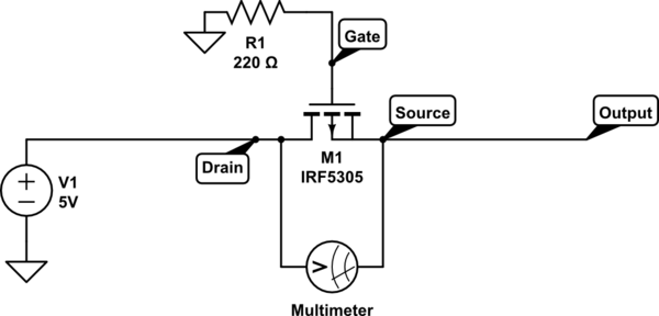
schematic

simulate this circuit – Schematic created using CircuitLab

\$\endgroup\$
11
  • 3
    \$\begingroup\$ Please show the circuit you're talking about. \$\endgroup\$
    – vofa
    Commented Jan 23, 2018 at 5:32
  • 1
    \$\begingroup\$ You apply 5V DC to the Drain and you get the output from Source. And the MOSFET is a P-Ch. one. Did I understand correctly? \$\endgroup\$ Commented Jan 23, 2018 at 5:51
  • 5
    \$\begingroup\$ "For clarity..." - for clarity you would have drawn a schematic. Your description of the circuit is ambiguous, and the operating conditions are unclear. 'larger than expected' and 'significant' are not measurements. \$\endgroup\$ Commented Jan 23, 2018 at 6:31
  • \$\begingroup\$ The GS threshold of MOSFETs is usually specified at a very small current. In case of IRF5305 it is specified at 250 uA. If you need to switch bigger current, you need to apply much higher GS voltage. \$\endgroup\$ Commented Jan 23, 2018 at 6:57
  • \$\begingroup\$ How are you measuring Rdson with your multimeter? Are you using your multimeter on resistance measurement, or are you drawing current through the MOSFET and measuring the voltage drop? \$\endgroup\$
    – marcelm
    Commented Jan 23, 2018 at 17:12

2 Answers 2

5
\$\begingroup\$

The RdsOn of .06 ohms specified for that mosfet is at Vgs = -10V. The Threshold voltage is where the mosfet starts conducting, not where it is fully saturated and RdsOn is at a minimum.

If you want to drive the gate at -5V you will need a logic level PFET.

\$\endgroup\$
3
  • \$\begingroup\$ I didn't realise it wouldn't be fully saturated at 5V. Does it mention on the datasheet the Vgs for saturation? How will I know if a different MOSFET is fully saturated at 5V? \$\endgroup\$
    – Jakkatak
    Commented Jan 23, 2018 at 23:10
  • \$\begingroup\$ doesn't Figure 1 of the datasheet indicate that for a Vgs of -5V, if the current from Drain to Source of the PMOSFET is less than 1A then the voltage drop from Drain to Source should be less than 0.1V? \$\endgroup\$
    – Jakkatak
    Commented Jan 23, 2018 at 23:20
  • \$\begingroup\$ @Jakkatak The word 'saturated' as you are using it applies to bipolar transistors only. A MOSFET is called 'saturated' when it limits current due to insufficient Gate voltage, whereas a bipolar transistor is 'saturated' when fully turned on. Seems silly to have two opposite meanings for a word, but there are reasons... \$\endgroup\$ Commented Jan 24, 2018 at 4:41
1
\$\begingroup\$

I have grounded the Gate through a pull-down resistor to discharge any gate capacitance between switching. I have connected a 5V DC power source to the Drain of the MOSFET, and there is a larger than expected voltage drop between Drain and Source of the MOSFET

You connect the 5 V DC between gate and source and not gate and drain. Then you measure resistance between source and drain. You have wired it incorrectly for your testing it seems.

It should turn on OK with only -5 volts gate to source.

\$\endgroup\$
3
  • 2
    \$\begingroup\$ Normally this would be true, but questioner wants to create an 'ideal diode' so Drain and Source must be swapped to prevent the body diode from conducting when the 'diode' is reverse biased. \$\endgroup\$ Commented Jan 23, 2018 at 13:36
  • \$\begingroup\$ @BruceAbbott I have only given instructions on how to test the MOSFET. Without more circuitry, extending my answer to debug something that does not appear to have been done yet is premature. \$\endgroup\$
    – Andy aka
    Commented Jan 23, 2018 at 14:35
  • \$\begingroup\$ @Andyaka, like Bruce Abbott says I need to connect the 5V to Drain for the body diode to operate in the desired direction. The 5V at drain will pass through the body diode, which will bias the MOSFET due to the positive voltage at Source and Gate grounded. I am then measuring the resistance between Drain and Source \$\endgroup\$
    – Jakkatak
    Commented Jan 23, 2018 at 23:00

Your Answer

By clicking “Post Your Answer”, you agree to our terms of service and acknowledge you have read our privacy policy.

Not the answer you're looking for? Browse other questions tagged or ask your own question.