11
\$\begingroup\$

We use them every day and those in the know fully understand the functional characteristics of BJT transistors. There are documents and links galore explaining the operational math. There are even tons of nice videos that explain current theories of how they physically work. ( Most of the latter given by folks that speak "Tele-marketer English" for some reason. )

However, I have to admit, even after 40+ years, a lot of it I have to accept at face value, since the descriptions of how the collector junction fits into the equation is always a bit hand-wavy.

Anyhow, that aside, there is one facet I really just don't get. It seems to defy the laws of physics, Kirchhoff's Laws et.al.

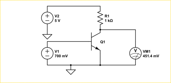
I'm talking about your standard saturated common emitter circuit.

It is known, and we accept, that when saturated, the collector voltage will be less than the base voltage. We obviously use that to our advantage in circuits and chose parts to give us as low a Vce-Sat as possible for a particular load current.

schematic

simulate this circuit – Schematic created using CircuitLab

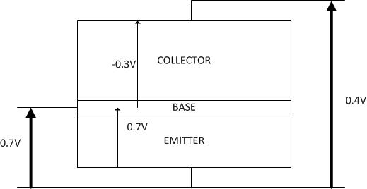
All fine and dandy, till you look at the quintessential mode of a typical NPN transistor...

enter image description here

How the heck can the collector be a lower voltage than the base in that sandwich?

Even if you add in some back-EMF type voltage in there to account for it, the collector current would be going the wrong way through the base-collector junction..

\$\endgroup\$
12
  • \$\begingroup\$ Does it help to think of the electrons as building momentum as they accelerate across Vbe, which carries them completely through the (very narrow) base region into the collector? (like freewheeling on your bike downhill and up the next (smaller) hill, missing the right turn onto a narrow track at the bottom? \$\endgroup\$
    – user16324
    Commented Feb 16, 2018 at 19:09
  • \$\begingroup\$ Looks like you might need to descend few levels of abstraction ... \$\endgroup\$
    – Eugene Sh.
    Commented Feb 16, 2018 at 19:10
  • \$\begingroup\$ @BrianDrummond ya that's the classical hand wavy answers I was talking about that bypass the basic laws of EE. That somehow they pop over without and Ohmic effect.. \$\endgroup\$
    – Trevor_G
    Commented Feb 16, 2018 at 19:14
  • 1
    \$\begingroup\$ Yeah. You have base emitter current. You have base collector current. And you have collector emitter current. The base collector current is low until you go into saturation. The reason base current increases (with Ic held constant) in saturation is that some of the current takes a shortcut to the base by going to the collector instead. \$\endgroup\$
    – user57037
    Commented Feb 16, 2018 at 19:15
  • 1
    \$\begingroup\$ It might be interesting to put a low value resistor between the collector and ground and measure how much current flows to ground through the collector vs. the expected path (through the grounded emitter). \$\endgroup\$ Commented Feb 16, 2018 at 20:01

6 Answers 6

6
\$\begingroup\$

In a bipolar transistor, the emitter has a much higher doping than the base. When you apply a forward bias to the base-emitter diode, current will flow, and due to the higher doping in the emitter, a lot more electrons flow from the emitter into the base than holes flow from the base into the emitter.

Current in a semiconductor can flow via two major mechanisms: There's "drift" current, where an electric field accelerates electrons in a certain direction. That's the simple way of current flow we're all used to. There's also "diffusion" current, where electrons move from areas of higher electron concentration into areas of lower concentration, much like water soaking into a sponge. However, those diffusing electrons can't move around forever since they will, at some point, hit a hole and recombine. That means diffusing (free) electrons in a semiconductor have a half-life and a so-called diffusion length, which is the average distance they travel before recombining with a hole.

Diffusion is the mechanism by which a diode junction creates its depletion region.

Now, if the base-emitter diode is forward-biased, the depletion region of the base-emitter diode gets smaller and electrons begin to diffuse from this junction into the base. However, since the transistor is built so that the diffusion length of those electrons is longer than the base is wide, a lot of those electrons are actually able to diffuse right through the base without recombining and come out at the collector, effectively "tunneling" through the base by not interacting with the holes there. (Recombination is a random process and doesn't happen immediately, which is why diffusion exists in the first place.)

So in the end, some electrons end up in the collector by random movement. Now that they are there, the electrons can only get back into the base when they overcome the forward bias voltage of the base-collector diode, causing them to "pile up" in the collector, decreasing the voltage there, until they can overcome the base-collector junction and flow back. (In reality, this process is an equilibrium, of course.)

With the voltages you apply to the base, emitter and collector, you only create the electric fields in the semiconductor that cause drift of electrons towards the depletion region, changing the concentration of electrons in the crystal, which then results in diffusion current flowing through the base. While single electrons are influenced by the electric fields created by the voltages at the transistor's terminals, they do not themselves have a voltage, only energy levels. Within a part of the crystal that is generally at the same voltage, electrons can (and will) have different energy. In fact, no two electrons can ever have the same energy level.

This also explains why transistors can work in reverse, but with much less current gain: It is harder for electrons to diffuse into the highly doped emitter region than into the lightly doped collector since the electron concentration is rather high there already. That makes this path less favorable for electrons than in the non-reversed transistor, so more electrons just flow straight out of the base and the gain is lower.
\$\endgroup\$
13
  • 1
    \$\begingroup\$ Jonathon, that is all very well, and classic, but it does not explain how you can have a layer in the middle that is at a higher voltage than the one above it. \$\endgroup\$
    – Trevor_G
    Commented Feb 16, 2018 at 19:33
  • \$\begingroup\$ @Trevor_G In a semiconductor, there aren't really "voltages". There are electric fields, but single electrons can have many different energy levels even though they're in the same area of the crystal. If that wasn't the case, there wouldn't be band gaps and therefore no semiconductors. An electron does not even have a voltage. \$\endgroup\$ Commented Feb 16, 2018 at 19:36
  • \$\begingroup\$ @JonathanS.: See my answer. Understanding the detail that Trevor is talking about requires an understanding that the fields/voltages associated with the base are not constant across its area, especially during saturation. \$\endgroup\$
    – Dave Tweed
    Commented Feb 16, 2018 at 19:48
  • \$\begingroup\$ I have read all this before, it still does not explain how the voltage can be lower at the collector, only how electrons make it through the depletion regions. Though you did briefly elude to tunnelling. \$\endgroup\$
    – Trevor_G
    Commented Feb 16, 2018 at 19:53
  • \$\begingroup\$ @Trevor_G The base is positively doped, the collector slightly negative. Since the base is small compared to the diffusion length of the electrons, we can assume an equal amount of electrons per area "lands" in the base and collector after diffusing. Since the collector is already negatively doped, it will have a larger concentration of electrons than the base, causing it to be at a lower voltage. \$\endgroup\$ Commented Feb 16, 2018 at 19:59
5
\$\begingroup\$

How the heck can the collector be a lower voltage than the base in that sandwich?

There's no law of physics that prevents the collector from being at a lower voltage than the base: apply \$0.7\,\mathrm{V}\$ between B and E, apply \$0.4\,\mathrm{V}\$ between C and E, and you'll bias the BJT in exactly that condition.

Therefore, your real question is probably: Given those applied voltages, how come that the law of physics allow the collector current to flow into the collector?

Kirchhoff's laws applied to the BJT imply only that $$-V_\mathrm{BE}-V_\mathrm{CB}+V_\mathrm{CE}=0$$ and $$I_\mathrm{C}+I_\mathrm{B}+I_\mathrm{E}=0,$$ where I assumed terminal currents as positive when entering into the terminals.

Furthermore, since there's no source of energy inside the BJT, we require the power entering the device to be positive (I consider a static case, neglecting dynamical effects to avoid the subtleties of passivity), that is, $$V_\mathrm{BE}I_\mathrm{B}+V_\mathrm{CE}I_\mathrm{C}>0.$$

These are the only constraints that physics puts on the terminal voltages and currents in the static case. As you can see, all the above conditions hold for a saturated BJT.

Your confusion probably comes from implicitly assuming a linear device, which a BJT is not.

\$\endgroup\$
15
  • \$\begingroup\$ Thanks for copying over your answer, I deleted the duplicate before your answer appeared sorry. \$\endgroup\$
    – Trevor_G
    Commented Feb 16, 2018 at 20:28
  • 3
    \$\begingroup\$ It appears that the origin of the confusion is assuming that current can only be a drift current. Diffusion current does not have to obey the electric field, actually it's the fact that it can flow despite an opposing electric field that make transistors capable of... transistor action. \$\endgroup\$ Commented Feb 16, 2018 at 21:58
  • 1
    \$\begingroup\$ @Trevor_G From your comments, I suspect that you think that the transport of electrons is driven by the electric field only, that is, the gradient of the electrical potential. Actually, what drives the electron transport is the electrochemical potential, which takes into account the inhomogeneity of the system, due to the varying carrier concentrations across the junctions. It's this inhomogeneity that generates the diffusion current. \$\endgroup\$ Commented Feb 17, 2018 at 12:32
  • 2
    \$\begingroup\$ @Trevor_G , As Massimo said, it's the gradient in concentration that gives rise to a diffusion current. Much in the same way a gas can expand upwards despite gravity. Electrons in a semiconductor are more like a gas (you can move them with a pump, but they can also move because of a concentration gradient) , while in a conductor they are more like a liquid (being incompressible, you need a pump to make it move). It appears to me you are asking: how can I have this gas move without a pump pushing in that direction? \$\endgroup\$ Commented Feb 17, 2018 at 14:32
  • 1
    \$\begingroup\$ Also, if somehow you managed to remove that diffusion current component, for example by placing a layer of conductor in the middle of the base, you would instantly 'condensate' that gas in a liquid, that by being swept out of the base would kill the transistor action. You'll end up with two diodes back to back, and in that case your objection on potentials would be valid. Problem is, you could not reach the same values of current and potentials you have in a transistor. \$\endgroup\$ Commented Feb 17, 2018 at 14:45
3
\$\begingroup\$

Keep in mind that the base does not have the same voltage throughout its area. There is an irreducible "sheet" resistance associated with the base, whose external connection must necessarily be at the edge of the structure in some sense. Since there is a current distribution within that "sheet", there is also a voltage distribution.

So, in saturation, the current that flows into the base terminal goes through both forward-biased diode junctions (B-E and B-C), near the base terminal. The current that went to the collector then flows to the emitter through a different part of the base that is farther away from the base terminal.

In essence, the voltage drop across the inherent base resistance is what allows the voltage distribution that we see at the external terminals.

\$\endgroup\$
2
  • \$\begingroup\$ Ya I though that might be something like that too, but then I realised if that were the case the farther away points would not be forward biased and not conducting, so the idea kind of falls apart. \$\endgroup\$
    – Trevor_G
    Commented Feb 16, 2018 at 19:46
  • \$\begingroup\$ No, it doesn't fall apart. There's no reason that some regions can't be forward biased while others are not. Stop thinking in terms of lumped circuit elements -- the fields vary continuously within a transistor, especially during saturation. The parts that are not forward-biased are functioning in the "classical" manner that Jonathan S. described. \$\endgroup\$
    – Dave Tweed
    Commented Feb 16, 2018 at 19:50
0
\$\begingroup\$

BJT's are current devices. When in the active region, lot's of the emitter's (emitters are heavily doped and more negative than the base) electrons go into the base (lightly doped) and some fall into the fewer base holes, but most diffuse across to the collector, causing Ic. When saturated, the collector is also more negative than the base, so it contributes some electrons to the base. As the collector contributes more electrons to the base (Vbc is more positive), it follows that collector-emitter current will be lower. As Vbc gets smaller (Vce(sat) is higher), the saturation current can be higher. So once in saturation, the collector voltage goes up with collector current.

You can run a transistor with the collector and emitter reversed. Since the collector is lightly doped compared to the emitter, gain is lousy, but Vce(sat) will be down in the single mV range. In the pre-FET era, we used this approach to ground analog inputs in sample-and holds, etc.

\$\endgroup\$
0
\$\begingroup\$

NON-RECTIFYING JUNCTION POTENTIALS. That's the trick.

Everyone's missing a simple, very basic fact. (Most beginner textbooks miss this too. Even some engineering profs seem clueless.) The fact: junctions always have a voltage across them, even when unpowered, even when it's metal-silicon with no diode effect ...and even when the junction is iron-copper, chromel-alumel, etc.

In other words, if we want to understand everything about diodes and transistors, we're not allowed to ignore thermocouple physics and NON-RECTIFYING JUNCTIONS. If we do, then Vce becomes unexplainable, a dark mystery of engineering.

[more to come]

\$\endgroup\$
-1
\$\begingroup\$

Ideally the Vbe matches the Vcb and both are forward conductng with Vce(sat)=0 at Imax and Ic/Ib=10.

As Dave T. pointed out the Vbe base spreading resistance (aka effective series R or ESR) is not uniform but by making multiple narrow base wells in parallel the performance improves.

When the ESR of the smaller higher doped B-E junction is higher than the larger ESR of the C-B junction we get a higher Vbe than Vcb thus Vce(sat) rises. THe current gain has now dropped to about 10% of max.

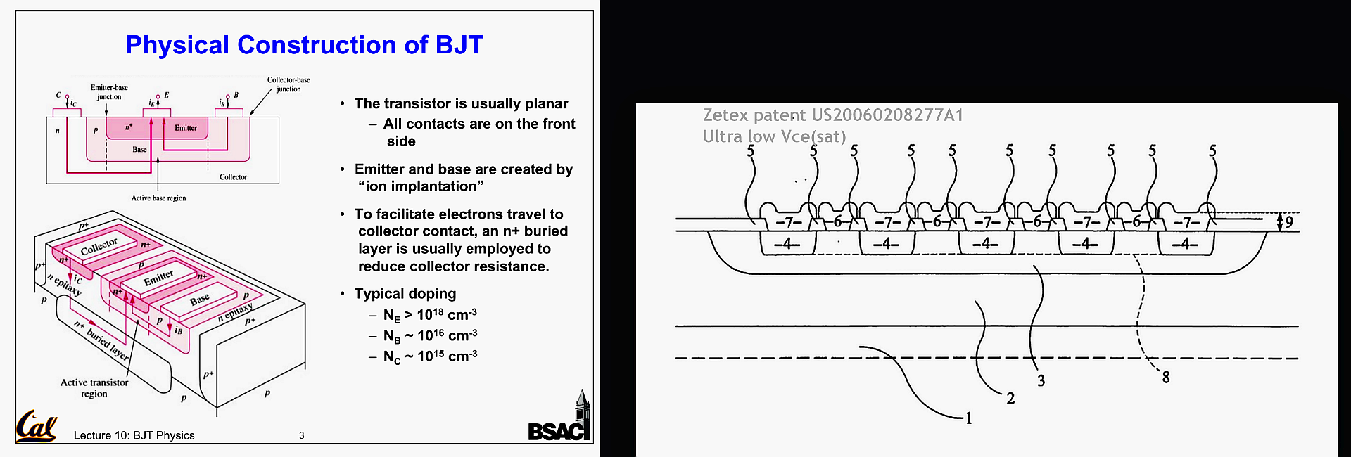
  • The epitaxial process is usually planar than vertical.
  • ion implantation is used for the emitter and base junctions.
  • the collector emittor current is increased thru a buried n+ layer to reduce the CE resistance or \$R_{CE}\$
  • many more electrons injcted into base than holes into emitter
  • since the base is made very narrow, most emitter electrons travel thru base and reach the collector

enter image description here

Zetex invented about 100 process patents around this epitaxial technology and now as Diodes Inc has many products although more expensive have similar dies sizes with Rce in the 10's of milliohms intead of obsolete TO-3 cans with Rce in the 1 Ohm range. This reduces the heat dissipation of at high currents significantly.

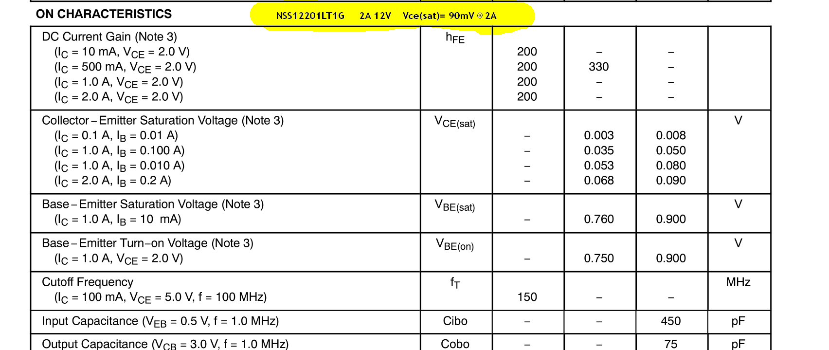
ON Semi have their own low Vce(sat) parts too.

This SOT-23 is <13 cents in volume and has Rce=45 mOhm max. Vce max= 12V

enter image description here

\$\endgroup\$
2
  • \$\begingroup\$ What is the problem? The base voltage creates the field for CE to conduct \$\endgroup\$
    – D.A.S.
    Commented Feb 18, 2018 at 4:02
  • \$\begingroup\$ No intelligent rebuttal -1 \$\endgroup\$
    – D.A.S.
    Commented Feb 18, 2018 at 18:55

Your Answer

By clicking “Post Your Answer”, you agree to our terms of service and acknowledge you have read our privacy policy.

Not the answer you're looking for? Browse other questions tagged or ask your own question.