My basic understanding of using a shift register to convert serial to parallel data is this:
- On every clock pulse, the state of the serial data pin is read
- As data is read, it gets shifted in to the registers
- When the latch pin pulses the values in the register are sent to the parallel output pins
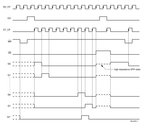
Here is a timing diagram for the 74HC595.

SH_CP is the clock, and DS is the serial data pin. To begin with DS is low, and then it goes high and then the latch starts pulsing... Then I don't really get it. As it stands I don't understand what this diagram explains or how it is useful to me.
