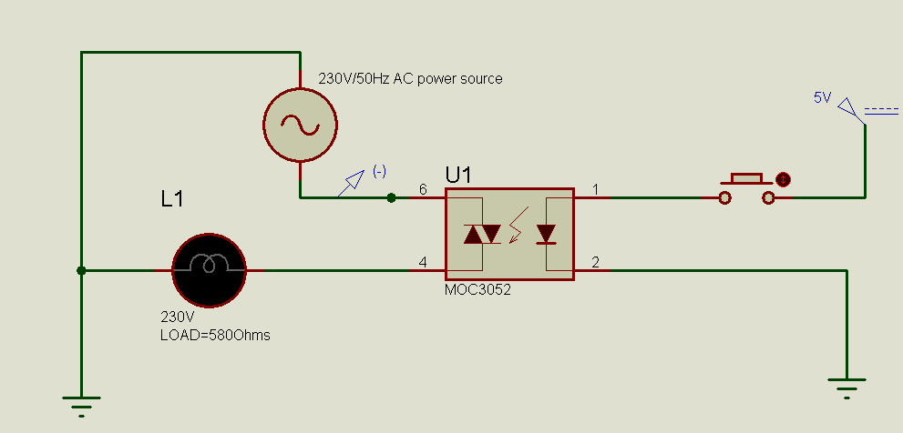
The ground connection on the left should not be be there. The whole point of the optoisolator is to provide galvanic isolation between the low voltage and mains sides.
It's also conventional to have signal flow from left to right, so normally the schematic should show the switch at the left and the output on the right. That's a style thing, it does not affect the actual circuit.
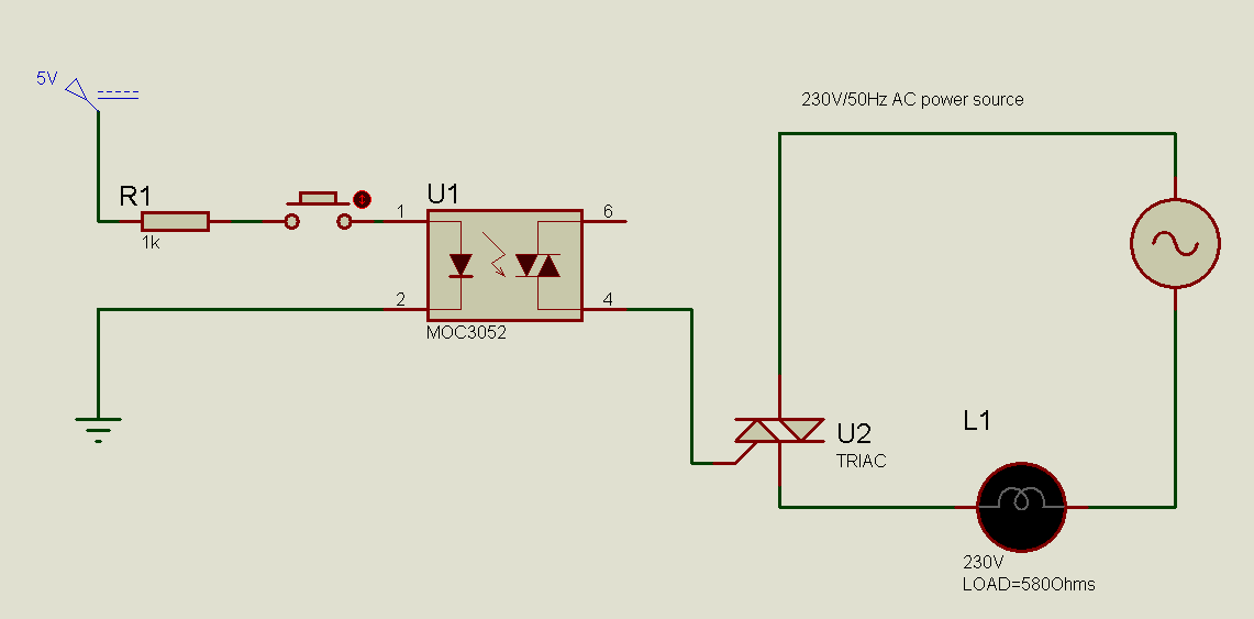
The input circuit has a problem- you will destroy the LED as soon as the switch is depressed since there is no series current-limiting resistor.
The output circuit has problems as well, the MOC3042 is not designed to switch a lamp load, it's main purpose is to switch a larger triac. If the incandescent bulb in your schematic is 100W and you have calculated the 580 ohms as the resistance, that is the resistance when it is hot. When you first apply power, the resistance will be much less, perhaps 1/10 to 1/20 of the resistance at operating temperature. That means that the current at switch-on could be in the 5-10A range, which could be enough to damage the device (the only hint is that the repetitive current is limited to 1A in the datasheet, and that will certainly be exceeded at times with such a load).
Even if it survives the initial turn-on, the power dissipation rating will be exceeded. See "Figure 2 On State Characteristics", and the maximum dissipation rating Pd of 150mW - 1.76mW/°C- which implies you should keep current to maybe 25mA to allow for moderately high ambient temperatures.
A small triac (8-16A range) will provide a lot more beefy ratings for switching a serious load, and the MOC3042 can be used to switch it. And don't forget the input resistor.


