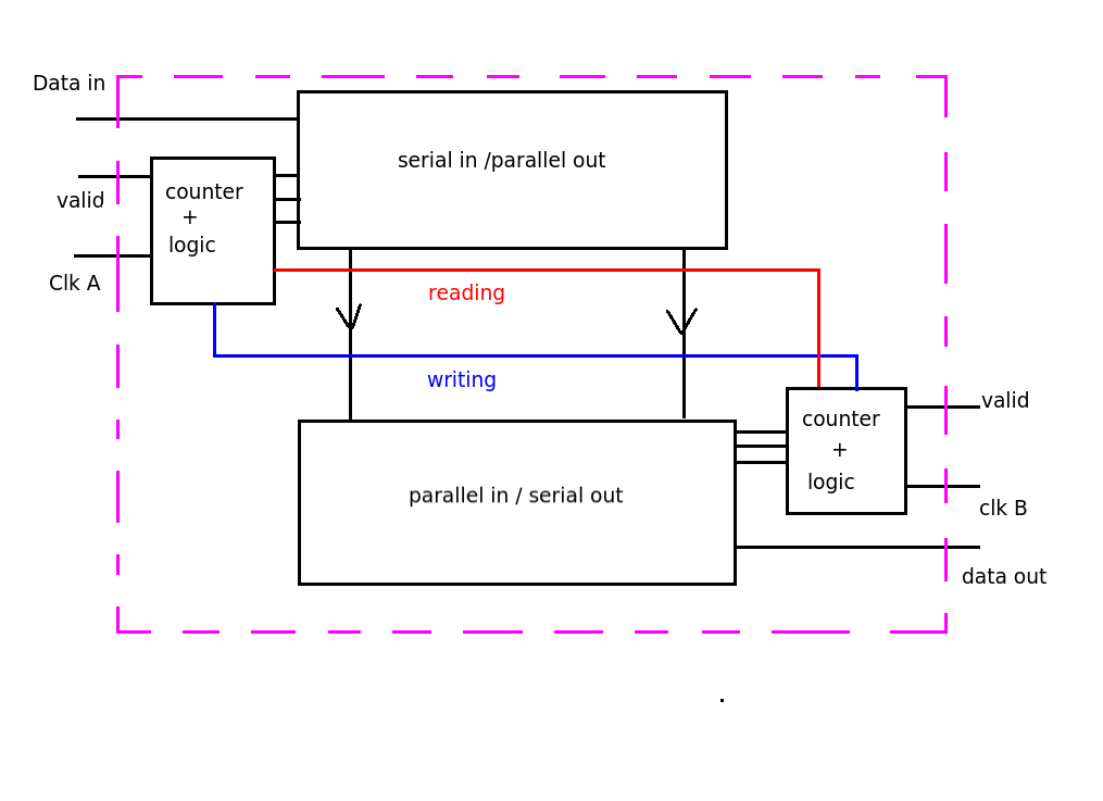
I think I'd have answered this interview question the same way you did. I believe the interviewer's requirement "to be done without a FIFO" was because a FIFO buffer is a valid, practical way to solve the problem of multiple clock domains -- but it can be done without the head/tail logic of a complete FIFO in many cases. And in the context of a job interview, simply instantiating a standard module doesn't demonstrate that you understand how to approach FPGA / HDL design. (I've interviewed candidates who couldn't even manage that small task.)
Passing data between different clock domains is usually done with three stages of flip-flops. The first stage is in the source clock domain (clkA), and the second and third stage flip-flops are in the receiver clock domain (clkB). The setup time of the second stage flip-flop is sometimes violated because the clocks are not synchronous, so the third-stage flip-flop is used to clean up the timing. Since there is a delay, the data_valid signal is passed in parallel with the data.
module SyncExample (
    input   wire            clkA,
    input   wire    [7:0]   Data_in,        // in clkA clock domain
    input   wire            Data_valid,     // in clkA clock domain
    input   wire            clkB,
    output  reg     [7:0]   Data_out,       // in clkB clock domain
    output  reg             Data_out_valid  // in clkB clock domain
    )

// First stage pipeline registers the clkA clock domain signals.
// pipeline_1_valid is set by Data_valid and remains set
// until cleared by pipeline_1_valid_clear acknowledge from clkB domain.
reg [7:0] pipeline_1_data;
reg       pipeline_1_valid;
wire      pipeline_1_valid_clear;
initial begin
    pipeline_1_data <= 0;
    pipeline_1_valid <= 0;
end
always @(posedge clkA) begin
    if (Data_valid) begin
        // capture pipeline_1_data only when Data_in is valid
        pipeline_1_data <= Data_in;
    end
    // keep pipeline_1_valid set after Data_valid, until pipeline_1_valid_clear.
    pipeline_1_valid <= (Data_valid | (pipeline_1_valid & ~pipeline_1_valid_clear));
end

// Second stage pipeline registers the clkB clock domain signals.
// Because clkA and clkB are asynchronous clock domains,
// setup time cannot be guaranteed for this stage.
// The previous pipeline_1 stage holds its data valid for
// more than one clkA cycle, to help achieve clkB setup requirement.
reg [7:0] pipeline_2_data;
reg       pipeline_2_valid;
initial begin
    pipeline_2_data <= 0;
    pipeline_2_valid <= 0;
end
always @(posedge clkB) begin
    pipeline_2_data <= pipeline_1_data;
    pipeline_2_valid <= pipeline_1_valid;
end

// Third stage pipeline registers the clkB clock domain signals.
initial begin
    Data_out <= 0;
    Data_out_valid <= 0;
end
always @(posedge clkB) begin
    Data_out <= pipeline_2_data;
    Data_out_valid <= pipeline_2_valid;
end

// pipeline_1_valid_clear timing feedback signals when the data-valid signal
// has propagated through all stages.
// For this simple example, we assume data_out is captured as soon as it is valid.
// A practical application should instead drive this with a read_data_out command.
assign pipeline_1_valid_clear = Data_out_valid;

endmodule;
You can also find similar example code in Xilinx ISE Language Templates under Verilog | Synthesis Constructs | Coding Examples | Misc | Asynchronous Input Synchronization.
edit:
Added pipeline_1_valid_clear signal and set/clear behavior to meet the slower clock domain's minimum pulse width requirement. Capture pipeline_1_data only when Data_in is valid.


