10
\$\begingroup\$

The below PCB belongs to a wireless access point.

Could anyone explain what are the golden-like part of the circuit that is indicated by the red circles(ish)? What material is it? What is the the functionality/use of it?
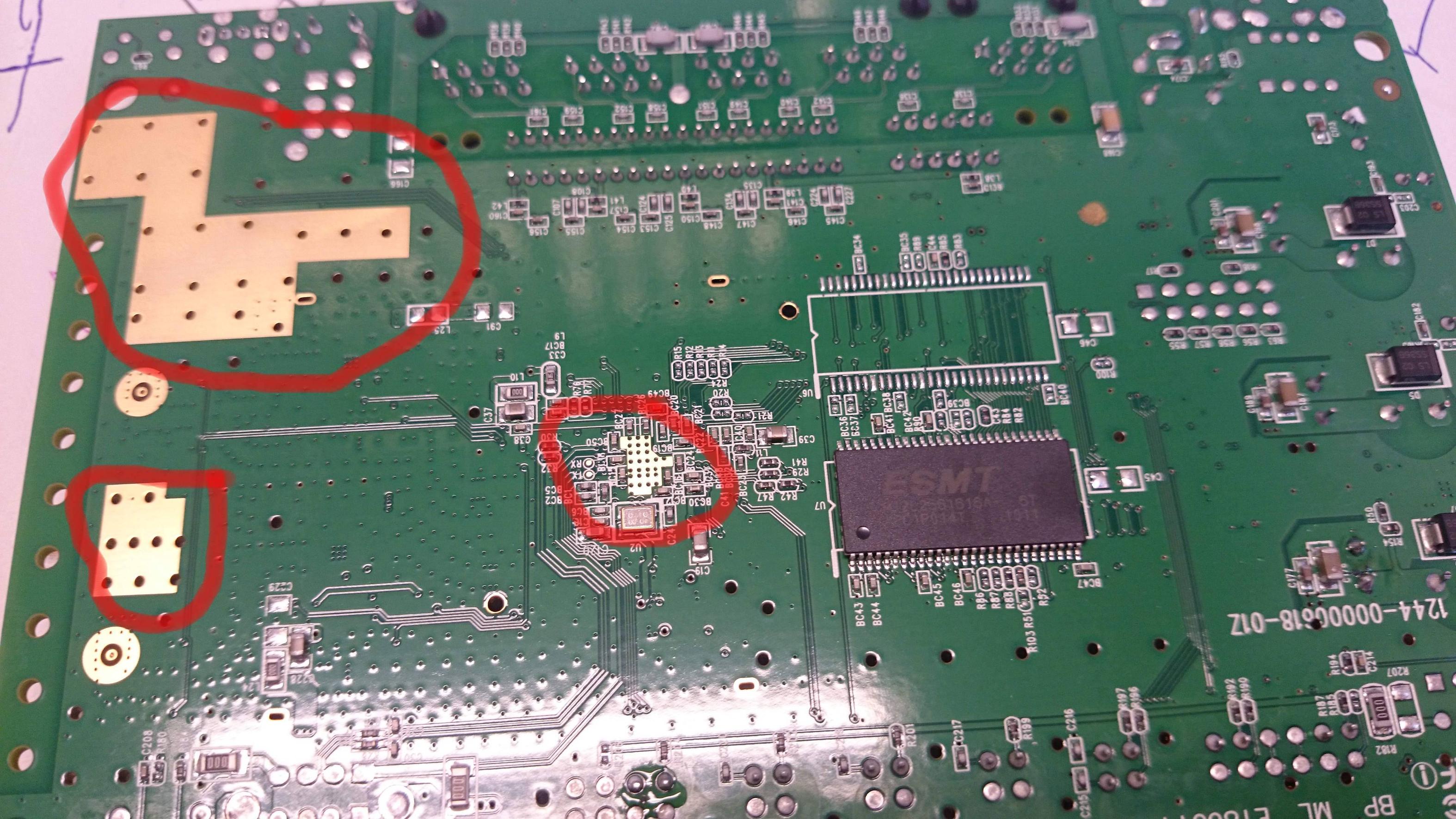
enter image description here

The left two circles have the same layout on the other side of PCB, and nothing is placed on top. The right circle is just under the wireless chipset.

P.S. I could not come up with a good title as I don't know the proper name or technique that is used on the PCB, please feel free to edit it.

\$\endgroup\$
1
  • \$\begingroup\$ I am thinking that it might be kind of a EMC shield or something to provide a better temperature performance as the right circle is just behind the chipset, but then the right part does not make much sense to me as there is nothing on that part \$\endgroup\$
    – Angs
    Commented Aug 21, 2014 at 11:08

3 Answers 3

16
\$\begingroup\$

The gold colour is just the surface finish of the PCB, called Gold Flashing.

The exposed areas could have a couple of uses:

  • As a grounding/earthing point, for example an RF screening gasket or can might make contact there.
  • Heat-sinking for a device. We have very similar footprints on boards for Allegro A4988 stepper motor driver chips and switch-mode power supply chips, but they can be anything that requires heat sinking.

There may be other reasons, those are the two I'm most familiar with.

Edit: Another reason is to do with RF performance or when RF devices such as filters or antennas are made purely using tracks on the PCB, in those cases the solder mask (and every other layer of the board) has an effect on the fabricated device, but I'm not an RF engineer so can't really expand on that other than being something I've seen in equipment we've designed.

\$\endgroup\$
1
  • \$\begingroup\$ Based on the sizes and shapes of these zones, and on the sizes and placement of the vias, these zones are likely heat sinks or heat sink attachment points. Note that solder resist (the green coating) is often not applied to copper pours that are designed to function as heat sinks; the solder resist coating would decrease the heat sink's thermal conductivity properties (the solder resist would restrict heat from being conveyed away from the underlying copper pour). \$\endgroup\$ Commented Jun 23, 2016 at 4:54
12
\$\begingroup\$

It looks like the exposed copper is gold plated. e.g. Wikipedia Electroless nickel immersion gold

That is a very common for SMD PCBs because it gives a lovely flat surface to solder SMD to.

Unlike other finishes, gold plating doesn't tarnish, or oxidise, so the PCB can be stored for months without it deteriorating.

\$\endgroup\$
1
  • 1
    \$\begingroup\$ Maybe the confusing part about the picture is this: The gold is visible in the unsoldered parts only. However, there is also gold underneath the solder joints, and likely on any copper area or trace, even under the green soldermask. So yes, it's just the finish, but most likely it's anywhere and not only in the exposed (unsoldered/unmasked) areas.. \$\endgroup\$
    – zebonaut
    Commented Jun 9, 2015 at 5:48
1
\$\begingroup\$

That plating is part of a process called ENIG, or Electroless Nickel Gold and it's purpose is to increase shelf life as stated in an earlier response. Also, it is flatter than other methods of finishing boards such as HASL (Hot Air Solder Leveling), which makes it more suitable for fine pitch SMD parts. This process step occurs after solder mask and is only applied to the exposed copper.

Fun fact: The gold is only a few microns thick and will "dissolve" into the solder when the board is reflowed.

\$\endgroup\$

Your Answer

By clicking “Post Your Answer”, you agree to our terms of service and acknowledge you have read our privacy policy.

Not the answer you're looking for? Browse other questions tagged or ask your own question.