4
\$\begingroup\$

I have included as much information as possible, so it should just be a matter of pointing out something simple (hopefully).

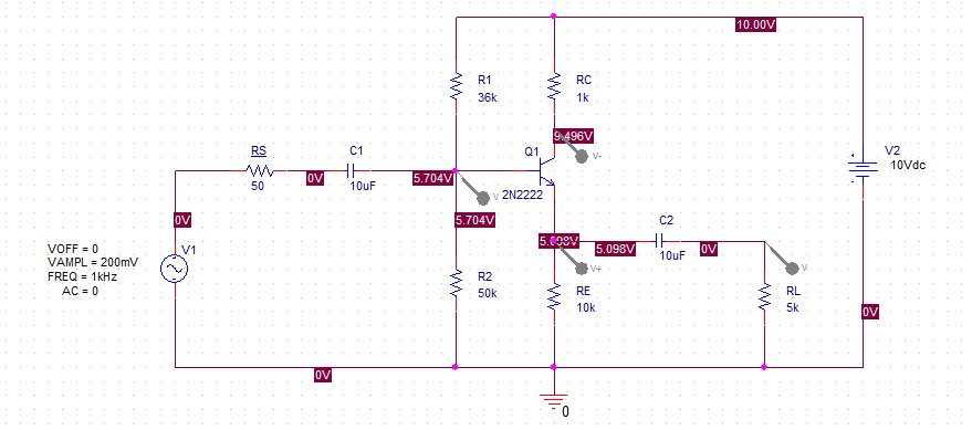
I am trying to model a biasing circuit for a Common Collector BJT Amplifier. I am running a Transient Analysis on the circuit and am receiving the following simulation results (attached images), which I am having trouble interpreting. I have also listed my minimum specs for the circuit and my theoretically computed values. As far as I can tell, I am doing everything correctly, although I am not seeing how to choose the Collector Resistance since it does not appear in any of my equations. I am also not seeing the voltage gain nor the Q-point as computed by PSPICE in the simulation Output File.

MINIMUM SPECS:

Input Resistance >= \$5\$k\$\Omega\$
Output Resistance = \$50\Omega\$
Voltage Gain \$\geq 0.95\$ with \$5\$k\$\Omega\$ load
Output Voltage Swing of at least \$2\$Vpp across \$5\$k\$\Omega\$ load
\$V_{cc} \leq 20\$V

FORMULAS USED:

Input Resistance: \$R_1 || R_2 || (\beta+1)R_E\$
Output Resistance: \$R_E || r_{\pi}/(\beta+1)\$
Voltage Gain: $$\frac{R_E(\beta+1)}{r_{\pi} + R_E(\beta+1)}$$
\$G_m\$: \$I_c/0.026\$
\$r_{\pi}\$: \$\beta/G_m\$

COMPUTED VALUES:

\$R_1\$: \$36k\Omega\$
\$R_2\$: \$50k\Omega\$
\$R_e\$: \$10k\Omega\$
\$R_c\$: ?
\$r_{\pi}\$: \$5075\$
\$g_m\$: \$0.0197\$
\$I_c\$: \$5.122 \times 10^{-4}\$
Voltage Gain: \$0.995\$
Vb: \$5.772\$V
Input Resistance >= \$20.5\$k
Output Resistance = \$50\$
Output Voltage Swing of at least \$2\$Vpp across \$5\$k load
\$Vcc \leq 10\$V

  • As you can see, I do not have a value for \$R_c\$, as I do not see how it affects any of my equations.


Circuit Image:


Simulation Waveform Image:


Simulation Waveform Cursor Values Image (Corresponds To Previous Waveform Image):


Simulation Output File:
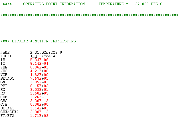
  • Where is the Q-POINT?
\$\endgroup\$
7
  • \$\begingroup\$ For a common collector the collector should be shorted to \$V_{CC}\$. Hence, \$R_{C} = 0\$. \$\endgroup\$
    – Null
    Commented Nov 17, 2014 at 1:50
  • \$\begingroup\$ My schematic suggests an unknown collector resistor, so my best guess was that it would not matter. But then why include it? Surely it must affect something. \$\endgroup\$
    – user58446
    Commented Nov 17, 2014 at 1:56
  • \$\begingroup\$ I suppose it's there to be general, but it is 0 for a true common collector circuit, by definition. You would include a collector resistor for a common emitter (output is at the collector) but for a common collector you don't care about the collector node (it's not in the signal path, and just needs to be at a high enough voltage that the transistors isn't in saturation) so you can tie it to \$V_{CC}\$. \$\endgroup\$
    – Null
    Commented Nov 17, 2014 at 2:00
  • \$\begingroup\$ So if Vb is 5.772V, my only concern with Rc is that Vc is greater than 5.722V, to function in forward-active mode? I do know that C>B>E is forward-active and C<B>E is saturation and C<B<E is cutoff. But these voltages we desire conflict with my understanding that the voltage across Rc is determine by the voltage bias across R1. How does this all come together? This may its own question... \$\endgroup\$
    – user58446
    Commented Nov 17, 2014 at 2:17
  • \$\begingroup\$ \$R_1\$ and \$R_2\$ set \$V_B\$, and then to make sure the transistor is in forward-active rather than saturation you need \$V_B < V_C\$. The voltage across \$R_C\$ is determined by \$I_C\$ since \$V_C = V_{CC} - I_CR_C\$. To set \$I_C\$, assume a diode drop (\$0.7\$V) for the BE junction, giving you \$V_E\$ from your \$V_B\$. Then set \$R_E\$ to give you the desired \$I_E \approx I_C\$. \$\endgroup\$
    – Null
    Commented Nov 17, 2014 at 3:51

1 Answer 1

3
\$\begingroup\$

"Common Collector" means that the Collector is a common point for both input and output signals (ie. Ground, or a fixed voltage relative to it). In a true Common Collector circuit the value of RC is zero Ohms. Larger values will still work, but with reduced output voltage swing.

In your circuit the Emitter can only go up to slightly less than 9V, because RC is then dropping 1V so the transistor is saturated (approaching zero volts between Collector and Emitter). However since you only need 2Vpp output and the quiescent Emitter voltage is ~5V, this should not be a problem.

\$\endgroup\$
5
  • \$\begingroup\$ Thank you for your feedback. It sounds like my circuit is biased correctly, aside from the Rc/V(swing) relationship. I'm not sure if you are familiar with PSPICE, but if you are: can you please point out on my Waveform and Cursor images where the Voltage gain can be observed, and where the Q-point is listed in the simulation Output File? The simulation results seem to indicate the voltages only for DC analysis, with capacitors as open. I have trying running an AC Sweep, but this creates more problems an is not how I am supposed to do this. \$\endgroup\$
    – user58446
    Commented Nov 17, 2014 at 2:24
  • \$\begingroup\$ DC analysis gives you the quiescent operating point (which is the state with no signal and all capacitors open). Transient analysis shows the instantaneous voltages vs time. Only AC analysis calculates signal amplitudes. To get gain you must run AC analysis and show output voltage divided by input voltage. \$\endgroup\$ Commented Nov 17, 2014 at 3:01
  • \$\begingroup\$ In the output file the Q-point is given as IC and VCE. The voltage gain can be derived from the emitter voltage display (amplitudes) divided by the input amplitude (200mV). And what are the problems connected with an ac analysis? \$\endgroup\$
    – LvW
    Commented Nov 17, 2014 at 7:08
  • \$\begingroup\$ Yes, thank you. I was not measuring the voltage gain correctly. I had too many voltage markers placed on the circuit and it was distorting the only two markers I needed. \$\endgroup\$
    – user58446
    Commented Nov 23, 2014 at 13:25
  • \$\begingroup\$ One last thing that is confusing me about saturation which you bring up regarding the <9V: I know this occurs when C<B>E. The problem is with the value of C. Is this determined by (Ic)x(Rc) or [Vcc - (Ic)(Re)]. They should be the same according to Mr. Kirchoff, except I see references to Vce = 0.2 which is used by the transistor across the Vce connection. So Vc may also equal [ V(e) + 0.2 ]. Should all these relationships equal the same? \$\endgroup\$
    – user58446
    Commented Nov 23, 2014 at 13:38

Your Answer

By clicking “Post Your Answer”, you agree to our terms of service and acknowledge you have read our privacy policy.

Not the answer you're looking for? Browse other questions tagged or ask your own question.