3
\$\begingroup\$

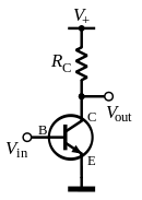
I've been trying to better understand BJT transistors. In particular I've been trying to understand the inverting amplifier configuration. Wikipedia shows this schematic:

commonemitter

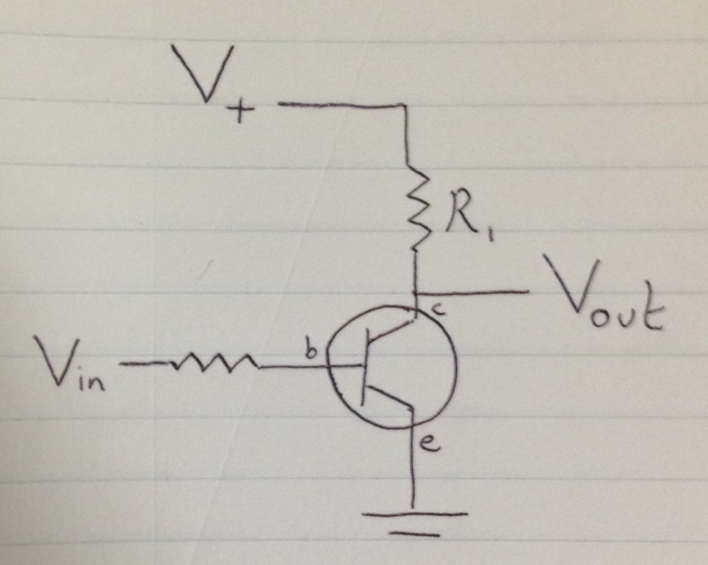
Which shows an input voltage Vin. However my understanding of how a BJT works tells me that there is effectively no resistance between the base and the emitter (is this correct?). This would mean an input from a voltage source would kill the BJT. And that it needs to be current limited like so:

commonemittercurrentlimit

I've written up my understanding in more detail here:

https://41j.com/blog/2014/12/npn-bjt-common-emitter-inverting-amplifier/

And tried to confirm experimentally, that there is no resistance between the base and the emitter. If there is an effective resistance between the base and the emitter, which parameter in the datasheet typically tells me what it is?

\$\endgroup\$

4 Answers 4

10
\$\begingroup\$

Understanding transistors is a bit like peeling an onion- there are many layers. At the simplest large-signal level you can consider the transistor as a current sink that's controlled by the current through the base-emitter junction. The latter behaves like a forward-biased diode. Not much current until you get to some hundreds of mV, and way too much current if you put volts across the junction. As you say, the transistor will conduct excessive current and will be destroyed if you simply connect (say) 5V to the base with emitter grounded. This is in stark contrast to the behavior of a MOSFET.

At a more sophisticated level of understanding (which is required if you want to predict how most amplifiers work) and for small signals the base-emitter junction behaves like a resistor of Vt/Ib where Vt is the thermal voltage, about 26mV at room temperature. So if your base current is 2.5uA (say the beta is 300 and the transistor is biased with 0.75mA collector current), the base-emitter junction looks like about a 10K resistor for small signals. You can consider the transistor as a (somewhat imperfect because of r0) voltage controlled current source with an input resistance of Vt/Ib. This is the hybrid-\$\pi\$ model. Note that the transconductance gm (and thus the voltage gain in a common emitter configuration) is a function of the collector bias current and temperature and beta does not enter into it at all.

http://en.wikipedia.org/wiki/Hybrid-pi_model

I must emphasize that this model is a linearized model about a bias point and is quite invalid if the (change in) input voltage is large (more than some millivolts). In other words we're talking about relatively small changes on top of a fixed base-emitter voltage of perhaps 600 or 700mV.

\$\endgroup\$
3
  • \$\begingroup\$ Thanks, this helped a lot. So as a rule of thumb, I can say that below 26mV the base to emitter junction will have some resistance? Are there parameters in transistor datasheets from which I can calculate at what levels I should take this resistance into consideration? I was looking at the 2N2222 datasheet in particular: 41j.com/blog/wp-content/uploads/2014/12/2N2222.pdf \$\endgroup\$
    – new299
    Commented Dec 11, 2014 at 15:42
  • \$\begingroup\$ The resistance I speak of is an approximation of the slope of a I-V plot of a diode curve. There is a bit of real resistance too (maybe ohms to tens of ohms), but that's another layer deeper. The base-emitter behaves much like a forward-biased diode. \$\endgroup\$ Commented Dec 11, 2014 at 17:51
  • 2
    \$\begingroup\$ "... below 26mV the base to emitter junction ...". Nope. The 26mV is kind of a magic number that never actually appears in the circuit -- it's just a number that appears in the math, and that happens to be useful for calculating the effective emitter resistance. Spehro left out the part of the "onion" analogy where you peel off a layer and then cry for a bit over all the new complications before steeling yourself and taking off another layer. \$\endgroup\$
    – TimWescott
    Commented Jan 3, 2020 at 17:08
2
\$\begingroup\$

If you realize that the current through a simple pn junction is a function of the applied voltage across the junction (exponential law) it is just a tiny logical step to accept that - of course - the same rule applies to the pn junction of a BJT. That´s what we have learned from W. Shockley and his famous equation. (In this respect you have to correct the corresponding parts of your text).

That means: If you really want to understand how and why the BJT functions, you must rely on the transconductance concept (voltage-controlled current source, transconductance gm). This was mentioned already in S. Pefhanys answer and the small-signal model he has given. But it is not only a "model" but it does reflect, indeed, the physical truth. There are several circuits as well as some observable effects which cannot be explained using the current-control concept.

Please, dont ask me why some textbooks speak about a current amplifier; I really have no explanation. Perhaps, because the equation Ic=B*Ib looks so nice and simple? Of course, during design of BJT circuits we have to use this relation because a currrent Ib does exist without any doubt. But this eqation does not tell anything about cause and effect. In fact, the current Ic (and as a small percentage of Ic) the current Ib both are caused and controlled by the voltage Vbe.

Back to one of your questions: Look onto the current-voltage characteristics of a pn diode. Of course, on each point of this curce you can define a ratio V/I (static resistance Rs for DC values) as well as a ratio v/i (differential resistance rd for small signal deviations). The same applies, of course, for the pn junction (base-emitter) of the transistor. As an important design parameter the small-signal resistance of the B-E junction is r,be=v,be/ib.

Because this is a differential quantity it can be expressed by the slope of the input characteristics. Differentiating the exponential function gives r,be=Vt/Ib=beta*Vt/Ic (Vt: Temperature voltage, Ib and Ic: DC currents). This value is - as you can see - dependent on the selected operational point; it is given for some typical values in the data sheet - typica values are in the lower kohm range. (The corresponding h-parameter is h11=hie).

Comment: The question "BJT current- or voltage controlled ?" was extensively discussed earlier - also in this forum (in 2013 if I am not wrong).
\$\endgroup\$
2
  • \$\begingroup\$ Thanks, your answer is as always very useful! I think this is the question you're referring to? electronics.stackexchange.com/questions/71144/… I will read through this. \$\endgroup\$
    – new299
    Commented Dec 11, 2014 at 16:03
  • \$\begingroup\$ Yes - but there was a similar discussion in this forum (also in 2013). Please ask in case you need some examples which support the voltage control explanation. \$\endgroup\$
    – LvW
    Commented Dec 11, 2014 at 16:22
1
\$\begingroup\$

A BJT basically consists of two diode junctions, one between BC and one between BE. You can crudely model it as a pair of diodes back to back.

enter image description here

There is no resistance in there, only the diodes.

\$\endgroup\$
6
  • \$\begingroup\$ Thanks, so would I be correct in assuming that if I drive the base with a voltage source I will kill the transistor unless I add an external resistor to limit the current? The wikipedia page appeared to suggest otherwise. \$\endgroup\$
    – new299
    Commented Dec 11, 2014 at 13:48
  • 1
    \$\begingroup\$ A BJT is a current amplifier. Without some form of control over the incoming base current you have no control over the collector current. The resistor converts a voltage into a current. \$\endgroup\$
    – Majenko
    Commented Dec 11, 2014 at 13:53
  • \$\begingroup\$ ok, thanks. If I've understood correctly the first schematic is therefore incorrect. \$\endgroup\$
    – new299
    Commented Dec 11, 2014 at 13:56
  • \$\begingroup\$ It depends to what use it is being put. Operated in saturation mode, i.e., a simple ON-OFF inverted switch (i.e., RTL NOT gate), then the current limit of whatever is driving Vin will be the controlling factor. It's certainly bad practice to stress an output by overloading its current like that. \$\endgroup\$
    – Majenko
    Commented Dec 11, 2014 at 13:58
  • \$\begingroup\$ Thanks again. For reference it's from here: en.wikipedia.org/wiki/Common_emitter it seems like Vin in figure 1, should probably be labeled Ib in this case. \$\endgroup\$
    – new299
    Commented Dec 11, 2014 at 14:02
1
\$\begingroup\$

The caption on the Wikipedia schematic says that it "[neglects] biasing details". This page has an example of a fully-biased common emitter amplifier, including a schematic:

Biased common emitter amplifier

This schematic features a resistor network to bias the base, as well as an emitter resistor. The emitter resistor is sometimes bypassed by a capacitor to increase AC gain. The base resistors are just an extra load on the signal source and don't affect the gain. So at AC, this schematic reduces to what you see on Wikipedia. From there, you can use the hybrid-pi model as Spehro discussed.

\$\endgroup\$

Your Answer

By clicking “Post Your Answer”, you agree to our terms of service and acknowledge you have read our privacy policy.

Not the answer you're looking for? Browse other questions tagged or ask your own question.