4
\$\begingroup\$

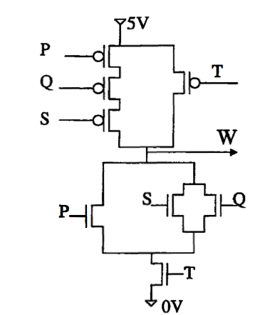
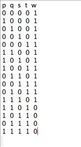
Hi can anyone help me figure out the truth table for this circuit? The output is w and the inputs are p, q, s, t. I have provided my answer for the truth table below, but I itit probably wrong.
enter image description here

enter image description here

Can someone explain to me how this works? I know in nmos 0 opens switch and 1 closes, and a pmos is the reverse of this. My problem is, I am not sure what happens if:

1) s & q are open (at the bottom)? Am i right in thinking if only one is open, w will be 0 providing p & t are shut (at the bottom)...

2) can current still flow if the top T is open? or in fact if any one of the top switches are open?

3) what will W be if current doesn't flow from bottom or top?

EDIT: OK I think I get it now. I basically end up with 9 5V outputs for w and the rest (7) 0V outputs. basically when T = 0, output will equal 1. When T = 1 output will equal 0 except for when PQS are open at the bottom (that is when PQS are all equal to 1).

Thanks for your help,

\$\endgroup\$
2
  • 1
    \$\begingroup\$ Smells like homework...... \$\endgroup\$ Commented May 25, 2011 at 2:02
  • \$\begingroup\$ notice that the top and bottom are complements of one another. the bottom section can pull W down if T is high, AND (P is high OR Q is high OR S is high); the top section pulls W up if T is low, OR (P is low AND Q is low AND S is low). This means W is always driven one way or the other, and you only need to look at half the circuit. Your truth table looks correct. \$\endgroup\$
    – JustJeff
    Commented May 25, 2011 at 23:04

2 Answers 2

2
\$\begingroup\$

The P, Q, S at the bottom form an OR gate; there's a path if either input is 1. But it's ANDed with T, so that W = 0 if (T = 1) AND (P = 1 OR Q = 1 OR S = 1). The top part is just the De Morgan dual of this: W = 1 if (T = 0) OR (P = 0 AND Q = 0 AND S = 0).
So W = NOT (T AND (P OR Q OR S)).

The P, Q, S at the bottom look more complicated than they are. They're drawn as P OR (Q OR S) but that's the same as (P OR Q OR S).

edit
Your truth table may be easier to interpret if you list the resp. inputs in binary counting order:

T P Q S
0 0 0 0
0 0 0 1
0 0 1 0
0 0 1 1
0 1 0 0
0 1 0 1
etc.

Some relationships between a certain input and the output may become more clear, in this case only in the bottom half of the table the output will be zero. The bottom half is when T = 1.

\$\endgroup\$
4
  • \$\begingroup\$ is there an eas way to spot which is 'and' and which is 'or' when looking at a circuit diagram? Going by what you say I cannot spot any mistakes in my answer... \$\endgroup\$
    – user559142
    Commented May 24, 2011 at 9:58
  • \$\begingroup\$ AND is when inputs are in series, OR is when they are in parallel. Think of light switches: the light is on if series switches A AND B are on, or when parallel switches C OR D are on. \$\endgroup\$
    – stevenvh
    Commented May 24, 2011 at 10:01
  • \$\begingroup\$ So in the top circuit, w can be 1 if either t is shut or p,q and s are shut? Also going by your above comment, isn't the top circuit then NOT((P AND S AND Q) OR T) \$\endgroup\$
    – user559142
    Commented May 24, 2011 at 10:04
  • \$\begingroup\$ the bottom half will not output zero if p q and s are 0 and t = 1 though will it? \$\endgroup\$
    – user559142
    Commented May 24, 2011 at 10:29
1
\$\begingroup\$

I didnt quite understand your question clearly. But I will try to answer from my limited knowledge. This circuit is based on CMOS logic. In this logic, PMOS is used as pull up and NMOS is used as pull down. That circuit is an implementation of ~[(P+Q+S).T] which is also can be written as
![(P | Q | S) & T] = (!P & !Q & !S) | T . Now lets answer your question.

  1. Yes, W will be pulled down. ie W will be 0V.
  2. In CMOS logic, current will flow only when the logic changes. That is only when W changes for 1 to 0 or when it changes from 0 to 1. Thats why CMOS is power efficient. When T switch is closed, W is pulled to Vdd.
  3. Like I explained for 2nd question, current will not flow always. W will just be pulled to Vdd or to Vss corresponding to the inputs applied.

Here in this circuit Vdd = 5V and Vss = 0V.

\$\endgroup\$
3

Your Answer

By clicking “Post Your Answer”, you agree to our terms of service and acknowledge you have read our privacy policy.

Not the answer you're looking for? Browse other questions tagged or ask your own question.