1
\$\begingroup\$

I have a comparator with open collector output (LM311) and a gate with open drain output (SN74LVC1G06). I want join these two outputs to make a wired-or, with a pull-up resistor tied to +3.3V.

In a general way, is it appropriate to join an open-drain output with an open-collector output?

\$\endgroup\$
1
  • \$\begingroup\$ Yes there's nothing wrong with doing that. Open-drain and open-collector are pretty much the same thing in this case. \$\endgroup\$
    – brhans
    Commented Jan 23, 2015 at 21:47

4 Answers 4

3
\$\begingroup\$

There really isn't an issue with that. Open drain and open-collector are essentially the same in this application.

Two things to watch out for:

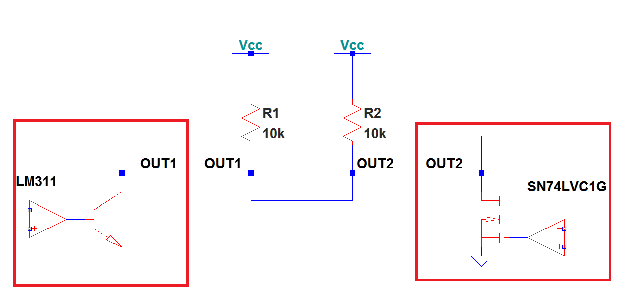
  1. Make sure you get your polarities right and that you need an OR gate and not a NOR gate because the open-collector/open-drain style often invert your signal. If the output of either opamp is high, then the output of that IC will be pulled low, and vice versa.

  2. Just make sure each IC can sink (Vcc/R1)+(Vcc/R2). This will be the worst case current if one output is low, and the other is high.

Picture for reference.

enter image description here

\$\endgroup\$
3
  • \$\begingroup\$ I read the question as having just the open-collector and open-drain wired directly together with a single pull-up resistor. No actual OR-gate required. \$\endgroup\$
    – brhans
    Commented Jan 23, 2015 at 21:46
  • \$\begingroup\$ @ACD I understand your point. I need an active-low OR, so a wired-OR could do the job (the output line goes low if any of the transistors goes low). My question is not about this specific application (is an example), but the compatibility of joining open-drain/collector outputs to make a active-low wired-OR. \$\endgroup\$ Commented Jan 23, 2015 at 21:49
  • \$\begingroup\$ @manu.argue I see now. Edited below the picture. \$\endgroup\$
    – ACD
    Commented Jan 23, 2015 at 21:57
4
\$\begingroup\$

Yes, you certainly can wire the two outputs together. Open drain and open collector just reflect the different technologies used inside the chips.

Keep in mind that 'wired or' is assuming input and output signals are inverted, so it's really an AND gate (both outputs must high-Z for the combined output to go high).

\$\endgroup\$
0
\$\begingroup\$

I am not sure if this concrete question and this practically oriented forum are the right place to reveal the philosophy behind the "wired OR" gate... but let me try... Here is my explanation why the "wired OR" really represents the OR logic function.

There is nothing special in this connection; actually it is the primary and most elementary OR gate. Only to see the OR logic function here, we have to think in terms of resistances, conductances or switch states.

From this point of view, the primary OR gate consists of elements (resistors, conductors or switches) connected in parallel that are driven by the input logical variables so that "conduct" (closed switch) represents "logical 1". It is obvious that, in this arrangement, the equivalent network will conduct (output logical 1) if only one of the elements conducts (input logical 1).

Dually, an AND gate consists of such elements connected in series. Now the equivalent network will conduct (output logical 1) if both the elements conduct (input logical 1).

Only electronic circuits use voltages (or more rarely, currents) as input and output variables. So, we should first convert the input voltages into resistances by some "electrically-controlled resistors" (FET, BJT, etc.), and then - the equivalent output resistance to voltage, by passing a current through it. The role of the pull-up resistor is just to provide this current.

NMOS logic gates are implemented exactly in this way. For example, an NMOS OR gate consists of NMOS transistors in parallel and a pull-up drain resistor. So, in this case we think of the whole combination as of an (N)OR gate including the transistors. The same is true in the case of RTL gate (the picture below).
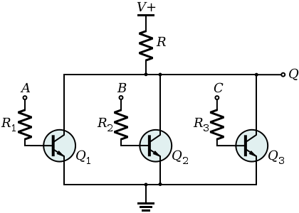
enter image description here

But what do we think in the case of a "wired OR"? What is the gate itself? In this case we do not consider the transistors as belonging to the logic gate... we consider them as external (belonging to the previous gates). And also, we do not consider the pull-up resistor as belonging to the logic gate... we consider it as external (belonging to the next gate).

But wait... what has remained then from our logic gate? Only a point, node, joined wires... that is why it is named "wired OR".

\$\endgroup\$
0
\$\begingroup\$

In a general way, is it appropriate to join an open-drain output with an open-collector output?

Yes (simple question, simple answer)

\$\endgroup\$

Your Answer

By clicking “Post Your Answer”, you agree to our terms of service and acknowledge you have read our privacy policy.

Not the answer you're looking for? Browse other questions tagged or ask your own question.