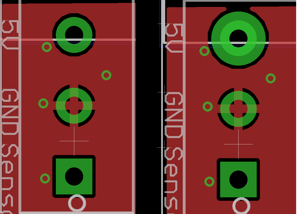
I wouldn't class myself as an expert on Eagle but I've recently been doing a fair amount of PCB design on it and I am always keen on trying to change the sizes of things without having to go into the footprint and alter things there.
However I found that there is no way to change the sizes of individual or in fact any holes / pads / vias that are there as part of a component footprint. You would have to go into the footprint and alter these things that you want but as you've said you don't want to do that - that's not very helpful.
I thought of a couple of different ways you could do what you want (depending on the reasons for you not wanting to change the footprint):
Modify and then re-name the footprint - If your reason for not changing the footprint is because you have other components that require the existing footprint then simply renaming it and modifying the bits you want will get around that issue. As you would just be making a new footprint but without all the hard work of starting from scratch, and you'd be able to keep the old footprint too.
Replace the footprint with individual vias - This could be an option as you would have control over the precise position and size of the hole / pad width. It would take a little bit of time to get everything in the right position but you could use the existing footprint as a sort of stencil and 'trace' over it and put your vias in exactly the same position. If you then grouped those components you could move them as a whole without upsetting the positioning of them relative to each other. Alternatively you could lock the components so that you can't move them by accident or without unlocking them first.
Note: With this method you would easily be able to alter the diameter / width of the pads once all the hard work was done in getting them to the right position was done.
- Talk to the manufacturer of the PCB - If by strengthen you mean that you want the copper layer to be thicker, you would have to talk to the PCB producer (if you're not doing it yourself) and you might be able to request that they use thicker copper layers - You probably won't be able to request individual pads to be of certain thickness and the others a different thickness but it could be worth a shot.
I have had issues with these pads ripping up. Never when trying to put the component in (although the holes were slightly too small and it needed some considerable force to get the component through) - my issues only ever come when trying to remove the component, I find I can never completely remove all the solder I have applied to the pins and end up trying to yank them out which just leads to the entire pad (both sides and through the middle) coming out with the pin! If you are against any of these ideas then there isn't really a lot that you can do, just be careful when assembling!


