0
\$\begingroup\$

I'm fairly new to electronics - I've had a reasonable amount of success with getting PCBs made using Eagle, but it was mostly wiring together breakouts and fairly simple stuff. I've spend the last two days learning about mosfets, resistors and transistors though, and one part of an existing circuit I'm using has me confused.

The LED being driven is a 5mm white 20mA. The existing schematic is here:
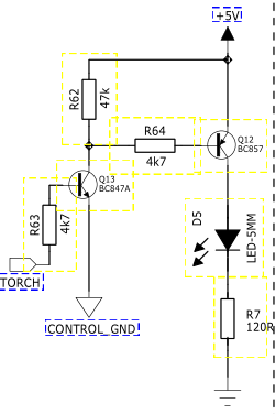
existing schematic

The PIC that is feeding "Torch" has an absolute maximum rating of 0.025A @ 3.3V [CORRECTED - previously stated 0.25A] on an IO pin (PIC16F1513). I don't understand why this simpler layout (on the right) wasn't used instead: enter image description here
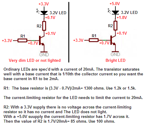
(picture taken from here: http://forum.allaboutcircuits.com/attachments/transistor-and-led-png.39778)

The question is: does the first circuit with two transistors have some advantage over the circuit with one transistor, given that the control is from a PIC?

[EDIT 2] The PIC datasheet is here: http://ww1.microchip.com/downloads/en/DeviceDoc/40001452D.pdf

\$\endgroup\$
2
  • \$\begingroup\$ I'm not quite sure what you are asking. Can you edit your question to make this more clear? \$\endgroup\$ Commented Feb 18, 2015 at 19:48
  • \$\begingroup\$ Hell, a single resistor directly driving the 20mA or less from the pin is all you really need. \$\endgroup\$
    – Passerby
    Commented Feb 18, 2015 at 23:42

3 Answers 3

2
\$\begingroup\$

Does the first circuit with two transistors have some advantage over the circuit with one transistor, given that the control is from a PIC?

If Vin was 12V, the PNP would conduct it to TORCH, destroying any 5V logic connected there. Adding the NPN allows an MCU, running at any voltage, to control the PNP, running at any other (usually much higher) voltage.

Conceptual schematic - additional, application-specific, bias resistors are required in most cases:

schematic

simulate this circuit – Schematic created using CircuitLab

(HIGH-SIDE, MCU-FRIENDLY) = (HIGH-SIDE) + (LOW-SIDE, MCU-FRIENDLY)

\$\endgroup\$
3
  • 1
    \$\begingroup\$ Just wanted to point out a terminology issue: you mentioned gate and drain to talk about a BJT in the third figure. \$\endgroup\$
    – Ricardo
    Commented Feb 18, 2015 at 23:04
  • 1
    \$\begingroup\$ The "schematic" was obviously intended to be conceptual, with no values or part numbers for anything. This isn't a game, so I'm not really here to "win votes"; I'm here to help the OP. If you are too, click "EDIT" and improve OUR best answer, wiki-style. \$\endgroup\$
    – Jon
    Commented Feb 19, 2015 at 0:23
  • \$\begingroup\$ @DwayneReid, I'll fix it as soon as I can read minds. Or, you could fix it, wiki-style, by clicking edit. \$\endgroup\$
    – Jon
    Commented Feb 19, 2015 at 7:32
3
\$\begingroup\$

The extra information does help.

The main difference between your 1st circuit and the right-hand lower circuit is how the load is connected. Your circuit is known as a "High-Side Switch", the lower circuits are known as "Low-Side Switches". The upper circuit also has more current gain than the lower circuits but that is important only when driving high-current loads.

Note that in both cases, the LED is turned ON when the input control signal is HI.

My preference is to use a Low-Side driver whenever possible. It has the advantage of lower component cost.

The lower circuits that you included in your question describe what happens if you use a supply voltage that is too low for your LED. A LED has a V-I curve where the LED conducts very little current below its' threshold voltage. When the threshold voltage is reached, the current increases rapidly with very little increase in voltage across the LED.

The left circuit is trying to show that: a 3.2V LED being fed from a 3.2V supply is just barely at the threshold point and doesn't draw much current. It is therefore quite dim.

The right circuit shows the LED operating with normal current and shows you how to calculate the resistor value needed to set the current through the LED.

\$\endgroup\$
2
  • \$\begingroup\$ +1 If the PIC is powered from +5 the high side switch need not be more complex or costly- simply connect R64 to the PIC rather than the Q13 collector and lose R62, R63 and Q13. Low = on then, of course, rather than the opposite. \$\endgroup\$ Commented Feb 18, 2015 at 21:04
  • \$\begingroup\$ Opps my mistake getting the transistor switching backwards. (I deleted my comment) Thanks for the correction Dwayne. \$\endgroup\$ Commented Feb 19, 2015 at 19:27
2
\$\begingroup\$

The two transistor circuit provides "high side drive" by switching the positive lead of the power supply, and allows the load to have one side grounded. In many cases this is highly desirable and in some cases it is essential.

Your two x 'one transistor' circuits are functionally identical - with the change from a 3.3V to 5V LED supply being extremely important in this case but not fundamental to the circuit operation in general terms.

Several of your claims are questionable. That's not meant to come across as rude - it's meant t help you learn.

You say

The PIC that is feeding "Torch" can handle 0.25A @ 3.3V on an IO pin (PIC16F1513)

This is extremely unlikely to be true if you mean that the PIC I/O pin can output 250 mA at 3.3 V under normal operation as defined in the specification sheet. Providing a link to a datasheet is always useful and, when you make specific claims, reference to the page and/or section in the datasheet may be useful.

You show the LED with 3.2V across it in both one transistor circuits but say it is dim or off i the lh cct and bright in the right. The description re brightness is likely to be correct and the statement re voltages is essentially certain to be wrong - IF this is the same LED then I_LED will be the same in both cases if V_LED is the same in both cases. Neither practice or theory are liable to give the comparative results that you show.
A white LED typically has ABOUT 3.2V drop at rated operating current (although white LEDS with operating voltages at rated current of from about 2.8V to 3.8V exist). The lh cct LED will be dim because as soon as any current is drawn the series resistor will drop some of the available voltage & the on transistor will drop some of the voltage and available LED voltage will be less than is needed for full current operation.

\$\endgroup\$
1
  • \$\begingroup\$ Ahh, you're right of course. That was my typo/bad maths! It's 25mA "absolute maximum rating". I've added the PIC's data sheet to the original question (p.g. 277 for the sink and source current limits). \$\endgroup\$
    – dannydc
    Commented Feb 19, 2015 at 10:48

Your Answer

By clicking “Post Your Answer”, you agree to our terms of service and acknowledge you have read our privacy policy.

Not the answer you're looking for? Browse other questions tagged or ask your own question.