4
\$\begingroup\$

Here is the datasheet of the crystal (32 MHz) that I use for a MCU.

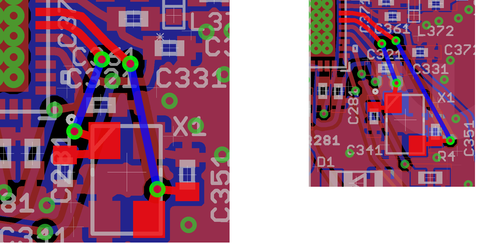
The right layout is an older version of my board which totally works fine. The left one is the newer version where I placed the components closer to each others (as well as the crystal). However, the 32 MHz crystal does not work properly on the new board ( I carefully assembled three of them).
enter image description here

I measured the pins of crystal by an oscillator, and I see the logic level of pins goes a higher, but don't oscillate. In addition, my code gets stuck on clock initialization.

Basically everything is the same, apart from the distance of the components.

What I did so far to debug the problem is that:

  • I replaced the crystal and load caps with the new ones and the ones from the old board that works for sure. It didn't help
  • pins of the crystals are measured by an oscillator, but there is no oscillation on the pins (the board has a 32k crystal as well, that one works fine).
  • I tested the same SW on different designs that the SW works correctly and it should be HW problem.
  • The orientation of the crystal is assembled correctly for sure, I use known brand capacitors (Murata and Kemet).
  • I inspected crystal's path to the MCU by a microscope and the solder on the pins looks fine.

Left side of CC321 bypass cap belongs to VCC path, and it might be too close to the crystal's In/Out pin (>0.2 mm). I wonder if it could be the problem that high frequency signal couples with the VCC path?

I removed the C321 but did not observe anything different.

Does anyone see any possible problem or have any suspicion or have any suggestion to debug/solve the problem?

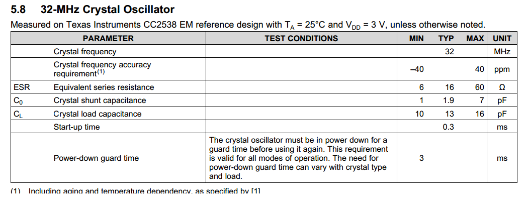
Additional information about the Crystal: enter image description here
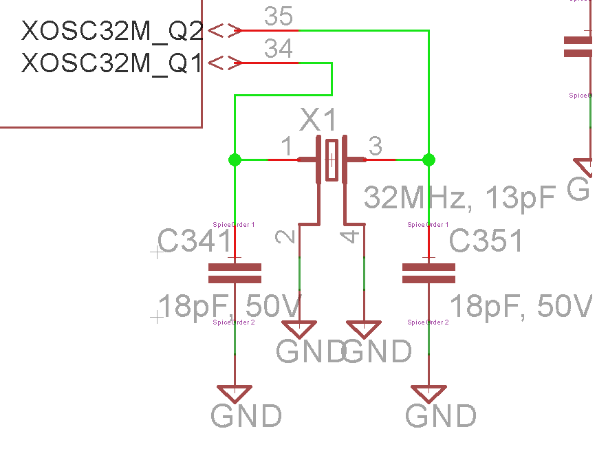
And related-schematic view of the layout
\$\endgroup\$
7
  • 2
    \$\begingroup\$ The spec you linked says 12pF for load capacitance then your picture says typically 13pF then you have 18pF on your circuit diagram (plus maybe 1 or 2pF from parasitic components). Try reducing your capacitors by a few pF and see what happens but, fundamentally your question appears to be anomalous on this matter. \$\endgroup\$
    – Andy aka
    Commented Feb 25, 2015 at 15:07
  • 2
    \$\begingroup\$ @Andyaka The load caps in a crystal osc are effectively in series, so he actually has 9pF + parasitics. As such its probably too low and I would suggest increasing them to 22pF or maybe even 27pF. \$\endgroup\$
    – brhans
    Commented Feb 25, 2015 at 15:12
  • 3
    \$\begingroup\$ Funny your schematic looks like the crystal inputs are actually grounded. What really happens internally with pins 3 and 4? Have you tried putting a 1Meg resistor across 1&3 sometimes you need a little something to get the oscillation started. \$\endgroup\$ Commented Feb 25, 2015 at 16:11
  • 2
    \$\begingroup\$ @Some Hardware Guy, Magically it worked:) But I can't understand why it worked, could you explain it as an answer? I couldn't understand why you said the input pins of crystal looks like grounded on the schematic? \$\endgroup\$
    – Angs
    Commented Feb 25, 2015 at 17:01
  • 1
    \$\begingroup\$ It is common practice to always place a 1Mohm resister in parallel to the crystal. Btw for EMC purposes I would recommend to move the crystal as close to the MCU pins as possible. This is one of your most important components to consider layout-wise, so move the passives to give room for it. \$\endgroup\$
    – Lundin
    Commented Feb 27, 2015 at 7:19

1 Answer 1

5
\$\begingroup\$

Hmm in meetings all day but maybe later or perhaps someone smarter will read this and give a good explanation hint hint. Basically the oscillator circuit is a little inverting amplifier with the input and output attached to the crystal. At time zero nothing is oscillating so it needs to be a little imbalanced to start oscillating. The 1Meg feedback resistor creates a little instability tying the output to the input. This starts the oscillation and then the crystal gets going.

Check out this link too

\$\endgroup\$
3
  • \$\begingroup\$ I soldered a throu hole resistor between pin 1 and 3. Do you see any way to fix the board without need of ordering new PCBs (My deadline is too soon)? \$\endgroup\$
    – Angs
    Commented Feb 25, 2015 at 17:22
  • \$\begingroup\$ May be putting a smd resistor on those two VIAS (over c364, the distance between them seens the same size the smd resistors you're using) is a good option? Or a very tiny resistor on IC's pads... \$\endgroup\$ Commented Feb 25, 2015 at 20:02
  • 1
    \$\begingroup\$ Maybe "no clean" solder was used and the leakage from the flux residue was too high to allow the oscillator to oscillate. \$\endgroup\$ Commented Feb 25, 2015 at 20:14

Your Answer

By clicking “Post Your Answer”, you agree to our terms of service and acknowledge you have read our privacy policy.

Not the answer you're looking for? Browse other questions tagged or ask your own question.