0
\$\begingroup\$

I'm trying to learn more about electronics. So to do that I decided to implement boolean logic gates in a circuit simulator. So far I have made NOT, AND, NOR and a S-R latch.

I wanted to try connect them together to make a S-R latch with only one input - a momentary switch.

My idea was that if you press the switch, the output of the S-R latch just flips. To do this I figured that if I take the output of the latch and AND it with the input of the button, I could take this signal to either the S or R input of the latch. And then for the other input I would AND the NEGATION of the output of the latch with the button.

Here are the circuits I made:
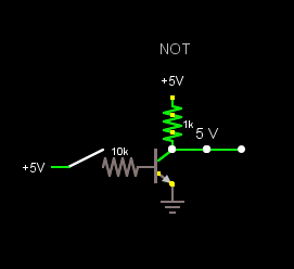
NOT gate:

not

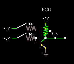
NOR gate:

nor

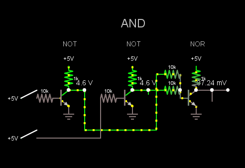
AND gate:

and

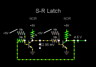
S-R latch:

latch

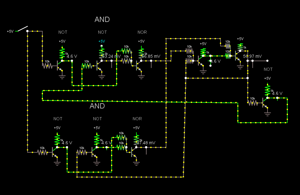
And finally the full circuit:

full

What seems to happen is when the momentary switch is pressed, both inputs of the latch are being pulsed which causes it to never flip over to the other state.

What can I modify or add to this circuit to make it work correctly?

\$\endgroup\$
0

2 Answers 2

1
\$\begingroup\$

If you look at the Truth Table for a S-R Latch, found here

wiki S-R Latch

you will see that the condition you are describing is "Not Allowed".

If you wish to have a circuit that toggles the outputs when both input are high you may want to consider a J-K Flip Flop; which is described further down on that same page.

\$\endgroup\$
2
  • \$\begingroup\$ I understand that the condition I am describing is not allowed. My question is how can I modify my circuit to stop that condition from happening in the first place? I could implement a J-K Flip Flop as you suggest, but I would like to understand what is wrong with my circuit first. \$\endgroup\$ Commented Mar 13, 2015 at 0:44
  • \$\begingroup\$ There is nothing "wrong" with your circuit, it is functioning as intended. If you want to "fix it" you would need to add a switch, then you would have one for "S"et and one for "R"eset. \$\endgroup\$
    – user69821
    Commented Mar 13, 2015 at 12:39
0
\$\begingroup\$

If you look at the first NOT gate closing the switch puts high voltage on the base relative to the emitter, current flows through the collector and voltage drops across the 1K resistor and the output is a low voltage. Overall a positive in gives a low out and if we define A TRUE as being a Positive voltage and that a Low voltage represents a FALSE condition you have in effect a NOT gate.

With the NOR gate if we define the TRUE and FALSE voltage representations as the same as above the true tabe for a NOR gate is that any TRUE on an input produces a FALSE on the output. In the circuit given if ether of the input switches are closed the transistor will pass Collector current and the output voltage will be low.So yes this will be a NOR gate. Note that if we define the output logic representation as TRUE represented by a LOW voltage then this same bit of circuitry is an OR gate.

This may seem confusing but its a fact that the representation of TRUES and FALSE is not written in stone a TRUE could be a high or a low voltage. One representation of this was by showing TRUE represented as a HIGH voltage by a solid line while TRUE represented by a LOW voltage by a dashed line.

\$\endgroup\$
2
  • \$\begingroup\$ Please parse your wall of text into smaller paragraphs that are related by content/context. As it is it is hard to understand in a clear manor, so it is likely not going to get any votes. Complex answers maybe best described by diagrams along with the text. \$\endgroup\$
    – user105652
    Commented Jul 2, 2016 at 22:12
  • \$\begingroup\$ @Viv: You need a double-Enter for a new paragraph. You had tried! \$\endgroup\$
    – Transistor
    Commented Jul 2, 2016 at 22:24

Your Answer

By clicking “Post Your Answer”, you agree to our terms of service and acknowledge you have read our privacy policy.

Not the answer you're looking for? Browse other questions tagged or ask your own question.