0
\$\begingroup\$

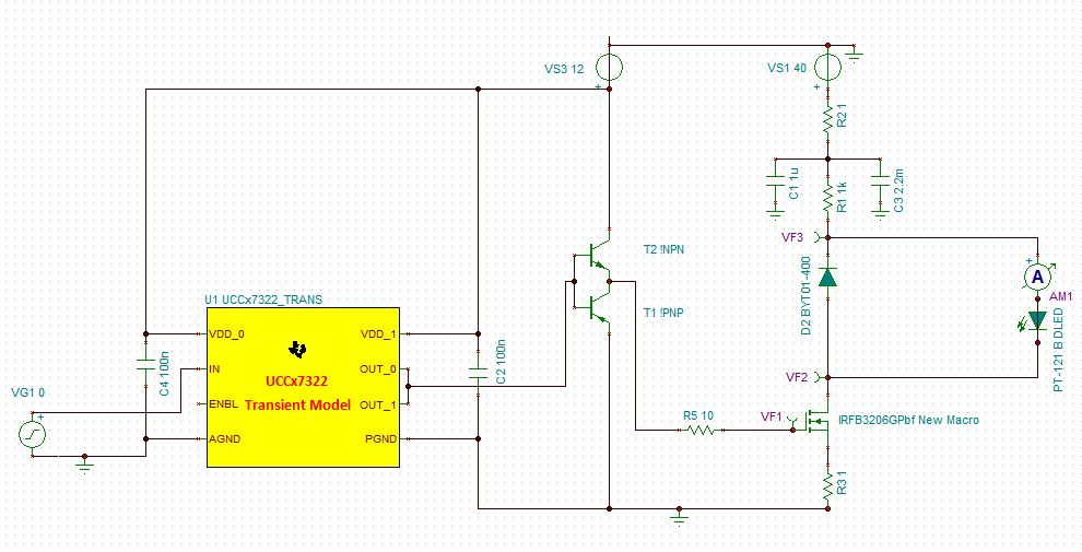
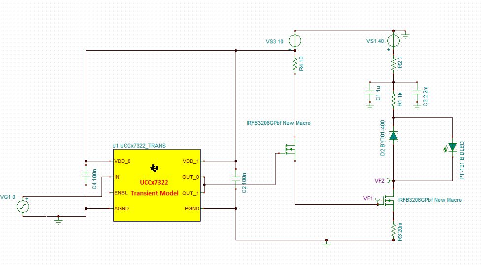
I have attached the following circuits which i have been developing overtime.

The OBJECTIVE is to get as high as possible a current at the gate of the MOSFET (VF1) to achieve faster pulse times of the LED.

My questions are:

-if there is any way to get higher currents at the MOSFET gate closest to the LED

-I am having trouble getting a higher voltage drop at the LED (VF2), adjusting the supply voltage VS1 has not contributed to increasing voltage across the LED

-the first circuit uses two mosfets and the second circuit uses an NPN/PNP BJT totem configuration to get higher current at the gate of the power MOSFET. Which of the two configurations should i pursue if my goal is to get faster switching at the MOSFET near the LED?

The circuit file is attached as well as the transient graphs. Any help/advice is welcome.enter image description here
enter image description here

\$\endgroup\$
1
  • \$\begingroup\$ Hmm. When you say the TI device has "limited the current at the gate", what values have you measured? What is the target current, and turnon time? You say "increasing voltage across the LED", but this voltage will always be the Vf of the LED and cannot be increased. \$\endgroup\$
    – pjc50
    Commented Mar 13, 2015 at 14:01

2 Answers 2

1
\$\begingroup\$

Method 1 has no gate pull down for the right hand MOSFET (Q2) so never turn it off properly.
The circuit could be modified to work properly, but the second circuit is easy and works well (when the error noted below is fixed).

In the lower circuit the PNP transistor should be inverted with collector to ground and emitter to output. The FET gate peak current is set by transistor capability and RS10. Depending on speed really required RS10 can be adjusted but usually 500 mA to 1A peak is adequate. What switching frequency do you require?

\$\endgroup\$
1
  • \$\begingroup\$ I shall consider your suggestions and get back to you with some specifics. work calls :) \$\endgroup\$
    – A Nilar
    Commented Mar 13, 2015 at 12:37
1
\$\begingroup\$

The first circuit won't work very well because the FET that receives the signal from the Texas device is in source follower mode and the source output voltage will be a couple of volts lower than the gate voltage. Also there is no pull-down resistor for when that first FET is turned off - this will likely leave the main power FET continuously turned on with its gate floating around. Eventually this may cause the power FET to become damaged due to heat.

Circuit 2 is better but you have shown two NPN transistors instead of a push-pull NPN-PNP pair. Assuming you meant NPN-PNP the drive voltage to turn the power FET on will be better than circuit 1 and this 2nd circuit will adequately turn-off the gate.

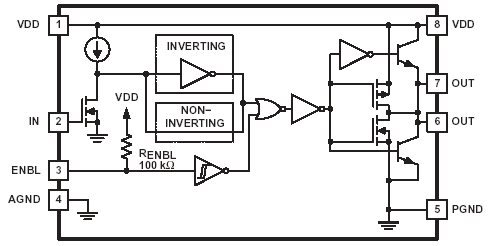
Why are you unable to drive the gate of the power FET directly from the Texas device? As far as I can tell the texas device has a push-pull output and will drive the power FET's gate directly: -

enter image description here

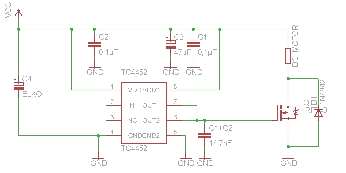
Here's a circuit of a similar device driving a motor via a single MOSFET: -

enter image description here

In other words, people are using it for similar applications without any extra silicon between the power FET and the Texas device.

\$\endgroup\$
1
  • \$\begingroup\$ thanks for the insight, to answer your question: directly driving the FET from the Texas Device has limited my current available at the gate. To achieve faster switching times, i realize i need to have higher current at the FET. My hunch was to use the second circuit and the answers here have confirmed my thoughts. The pait of BJTs are NPN-PNP pair as available on TINA-TI. I was unsure of the circuit symbol as well but it is what is available. I shall upload some transient graphs later in the day. Hopefully clarifying my intentions. \$\endgroup\$
    – A Nilar
    Commented Mar 13, 2015 at 12:33

Your Answer

By clicking “Post Your Answer”, you agree to our terms of service and acknowledge you have read our privacy policy.

Not the answer you're looking for? Browse other questions tagged or ask your own question.